Datasheet Details
| Part number | SN74LVC74A-Q1 |
|---|---|
| Manufacturer | Texas Instruments |
| File Size | 827.01 KB |
| Description | Dual Positive-Edge-Triggered D-Type Flip-Flops |
| Datasheet |
 SN74LVC74A-Q1-etcTI.pdf SN74LVC74A-Q1-etcTI.pdf
|
| Part number | SN74LVC74A-Q1 |
|---|---|
| Manufacturer | Texas Instruments |
| File Size | 827.01 KB |
| Description | Dual Positive-Edge-Triggered D-Type Flip-Flops |
| Datasheet |
SN74LVC74A-Q1-etcTI.pdf
|
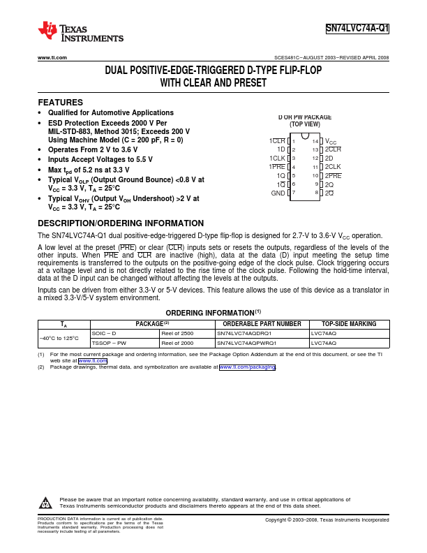
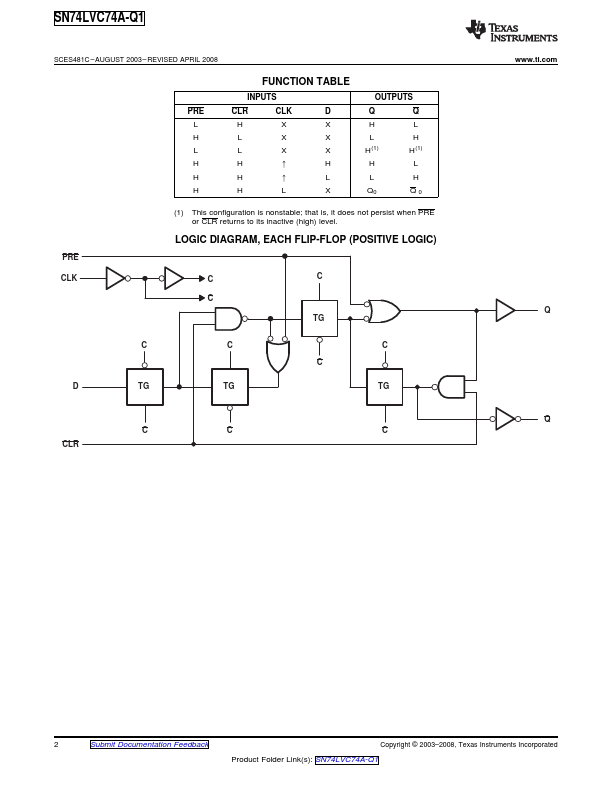
ORDERING INFORMATION The SN74LVC74A-Q1 dual positive-edge-triggered D-type flip-flop is designed for 2.7-V to 3.6-V VCC operation.A low level at the preset (PRE) or clear (CLR) inputs sets or resets the outputs, regardless of the levels of the other inputs.When PRE and CLR are inactive (high), data at the data (D) input meeting the setup time requirements is transferred to the outputs on the positive-going edge of the clock pulse.Clock triggering occurs at a voltage level and is not directly
📁 SN74LVC74A-Q1 Similar Datasheet