AAT3119 Overview
Key Features
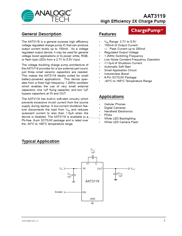
- ChargePump™ VIN Range: 2.7V to 5.5V 150mA of Output Current
- supply during startup. A low-current shutdown fea
- ture disconnects the load from VIN and reduces
- quiescent current to less than 1.0μA when the
- device is disabled. The AAT3119 is available in a
- Pb-free, 8-pin SC70JW package and is rated over
- the -40°C to +85°C temperature range