Power supply voltage pin Thermistor connection pin Input pin for resonance circuit voltage Input pin for resonance circuit power supply voltage Output pin for status display Resistor connection pin for tON time setting GND pin FET gate drive pin for resonance
4
Rev.1.2_00
WIRELESS POWER TRANSMITT
Key Features
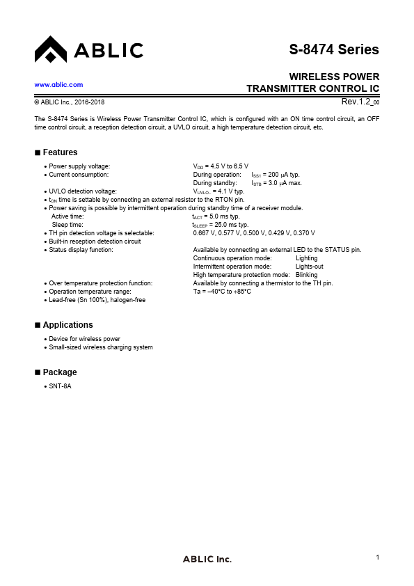
Power supply voltage:
VDD = 4.5 V to 6.5 V.
Current consumption:
During operation: ISS1 = 200 A typ. During standby: ISTB = 3.0 A max.
UVLO detection voltage:
VUVLO = 4.1 V typ.
tON time is settable by connecting an external resistor to the RTON pin.
Power saving is possible by intermittent operation during standby time of a receiver module. Active time:
tACT = 5.0 ms typ. Sleep time:
tSLEEP = 25.0 ms typ.
Full PDF Text Transcription for S-8474 (Reference)
Note: Below is a high-fidelity text extraction (approx. 800 characters) for
S-8474. For precise diagrams, and layout, please refer to the original PDF.
The S-8474 Series is Wireless Power Transmitter Control IC, which is configured with an ON time control circuit, an OFF time control circuit, a reception detection circuit, a UVLO circuit, a high temperature detection circuit, etc. Features Power supply voltage: VDD = 4.5 V to 6.5 V Current consumption: During operation: ISS1 = 200 A typ. During standby: ISTB = 3.0 A max. UVLO detection voltage: VUVLO = 4.1 V typ. tON time is settable by connecting an external resistor to the RTON pin. Power saving is possible by intermittent operation during standby time of a receiver module. Active time: tACT = 5.0 ms typ