ACE Technology ACE2607B
ACE2607B is produced with high cell density, DMOS trench technology, which is especially used to minimize on-state resistance. This device particularly suits for low voltage application such as portable equipment, power management and other battery powered circuits, and low in-line power loss are needed in a very small outline surface mount package. The value of PD is measured with the device mounted on 1in 2 FR-4 board with 2oz.| Part No. | ACE2607B |
|---|---|
| Datasheet | ACE2607B Download |
| Manufacturer |  ACE Technology |
| Description | P-Channel Enhancement Mode Field Effect Transistor |
| Buy | Stock & Price |
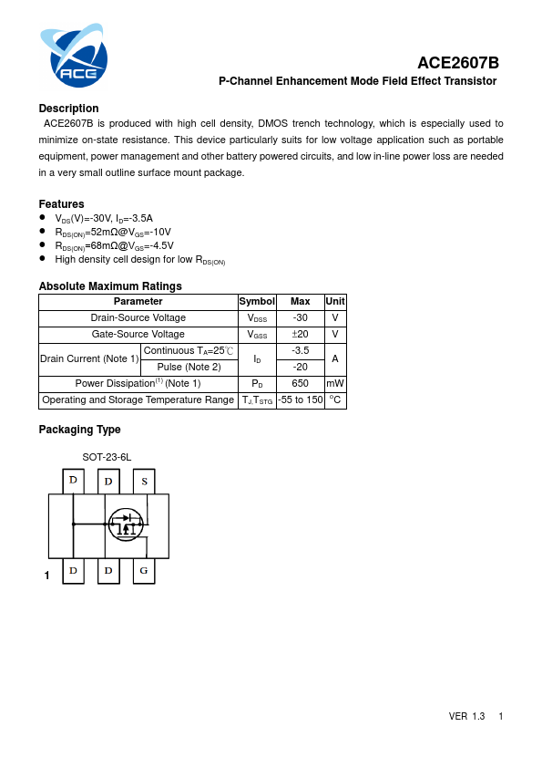
DESCRIPTION
FEATURES
● VDS(V)=-30V, ID=-3.5A● RDS(ON)=52mΩ@VGS=-10V
● RDS(ON)=68mΩ@VGS=-4.5V
● High density cell design for low RDS(ON)
ABSOLUTE MAXIMUM RATINGS
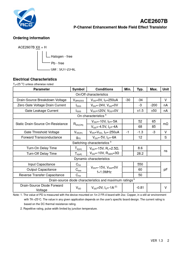
Parameter Symbol Max Unit Drain-Source Voltage VDSS -30 V Gate-Source Voltage VGSS ±20 V Drain Current (Note 1) Continuous TA=25℃ Pulse (Note 2) ID -3.5 A -20 Power Dissipation(1) (Note 1) PD 650 mW Operating and Storage Temperature Range TJ,TSTG -55 to 150 OC Packaging Type SOT-23-6L 1 VER 1.3 1 ACE2607B P-Channel Enhancement Mode Field Effect Transistor Ordering information ACE2607B XX + H Halogen - free Pb - free GM : SOT-23-6LELECTRICAL CHARACTERISTICS
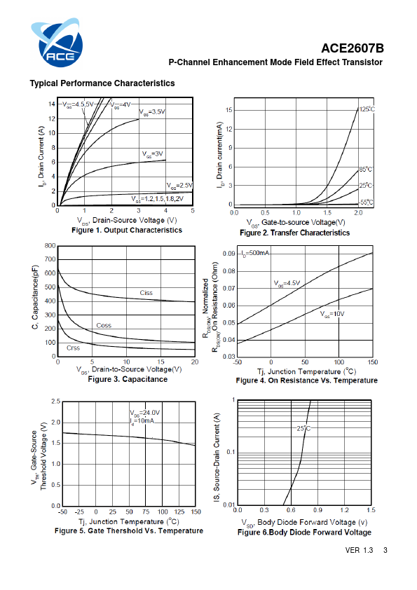
TA=25 OC unless otherwise noted Parameter Symbol Conditions Min. Typ. Max. Unit On/Off characteristics Drain-Source Breakdown Voltage V(BR)DSS VGS=0V, ID=250uA -30 -34 V Zero Gate Voltage Drain Current Gate Leakage Current IDSS VDS=-24V, VGS=0V IGSS VGS=±20V, VDS=0V On characteristics b -3 ±1.5 -200 ±50 nA nA Static Drain-Source On-Resistance Gate Threshold Voltage RDS(ON)...