ADM15P06D
ADM15P06D is P-Channel MOSFET manufactured by ADV.
P-Channel Logic Level Enhancement Mode Field Effect Transistor
PRODUCT SUMMARY
VDSS -60V
ID -15A
RDS(ON) (mΩ) 90mΩ
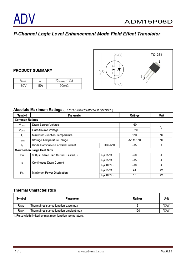
TO-251 2
1...
| Part Number | Description |
|---|---|
| ADM15P06E | P-Channel MOSFET |
| ADM15N03S | N-Channel MOSFET |
| ADM100N10 | N-Channel MOSFET |
| ADM105N03E | N-Channel MOSFET |
| ADM12N03S | N-Channel MOSFET |