Click to expand full text
ADV
ADM3N06B
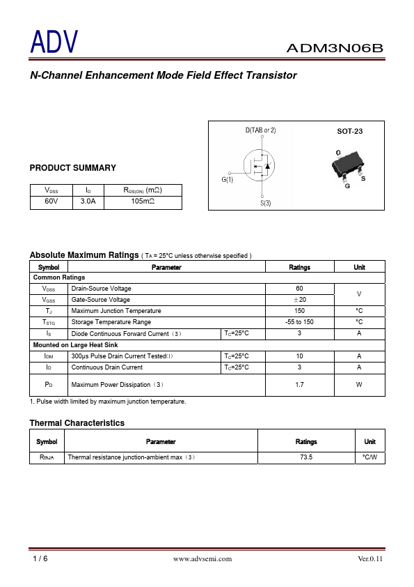
N-Channel Enhancement Mode Field Effect Transistor
PRODUCT SUMMARY
VDSS 60V
ID 3.0A
RDS(ON) (mΩ) 105mΩ
SOT-23
Absolute Maximum Ratings ( TA = 25°C unless otherwise specified )
Symbol
Parameter
Common Ratings
VDSS
Drain-Source Voltage
VGSS
Gate-Source Voltage
TJ
Maximum Junction Temperature
TSTG
Storage Temperature Range
IS
Diode Continuous Forward Current(3)
TC=25°C
Mounted on Large Heat Sink
IDM
300μs Pulse Drain Current Tested⑴
ID
Continuous Drain Current
TC=25°C TC=25°C
PD
Maximum Power Dissipation(3)
1. Pulse width limited by maximum junction temperature.
Thermal Characteristics
Symbol
Parameter
RthJA Thermal resistance junction-ambient max(3)
Ratings 60 ±20 150
-55 to 150 3
10 3 1.7
Ratings 73.