The following content is an automatically extracted verbatim text
from the original manufacturer datasheet and is provided for reference purposes only.
View original datasheet text
ADV
ADM4N06A
N-Channel Enhancement Mode Field Effect Transistor
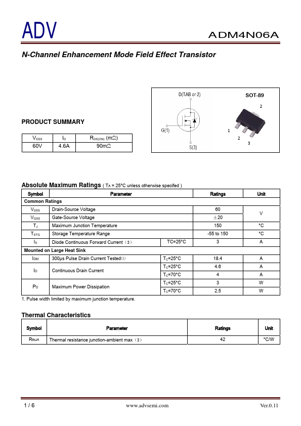
PRODUCT SUMMARY
VDSS 60V
ID 4.6A
RDS(ON) (mΩ) 90mΩ
SOT-89
2
1 2 3
Absolute Maximum Ratings ( TA = 25°C unless otherwise specifed )
Symbol
Parameter
Common Ratings
VDSS
Drain-Source Voltage
VGSS
Gate-Source Voltage
TJ
Maximum Junction Temperature
TSTG
Storage Temperature Range
IS
Diode Continuous Forward Current(3)
TC=25°C
Mounted on Large Heat Sink
IDM
300μs Pulse Drain Current Tested⑴
ID
Continuous Drain Current
PD
Maximum Power Dissipation
1. Pulse width limited by maximum junction temperature.
TC=25°C TC=25°C TC=70°C TC=25°C TC=70°C
Thermal Characteristics
Symbol
Parameter
RthJA Thermal resistance junction-ambient max(3)
Ratings
60 ±20 150 -55 to 150
3
18.4 4.6 4 3 2.