AFSEMI SSC8313GS1
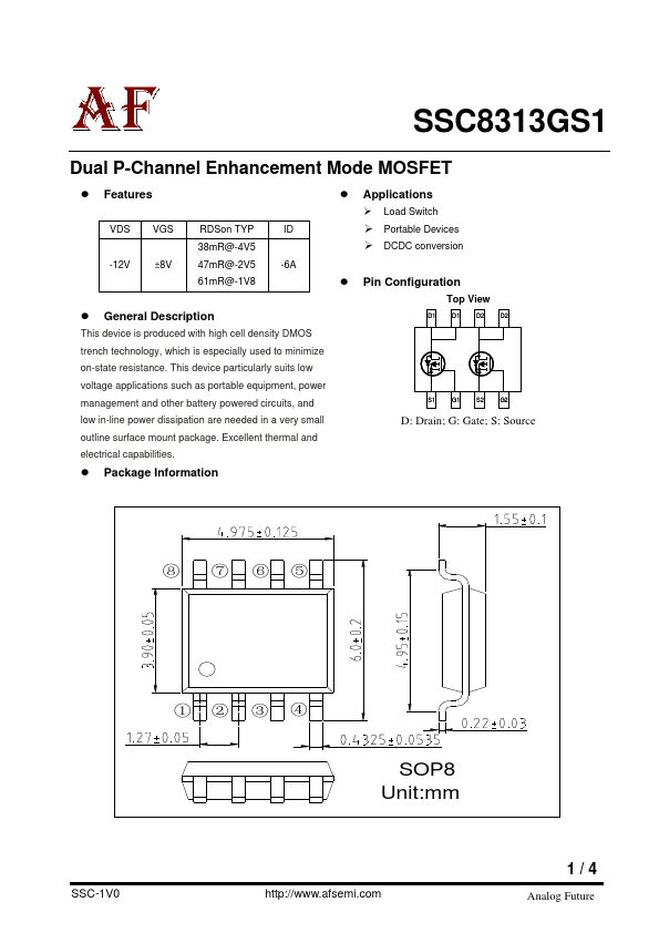
This device is produced with high cell density DMOS trench technology, which is especially used to minimize on-state resistance. This device particularly suits low voltage applications such as portable equipment, power management and other battery powered circuits, and S1 G1 S2 G2 low in-line power dissipation are needed in a very small D: Drain; G: Gate; S: Source outline surface mount package.| Part No. | SSC8313GS1 |
|---|---|
| Datasheet | SSC8313GS1 Download |
| Manufacturer | AFSEMI |
| Description | Dual P-Channel Enhancement Mode MOSFET |
| Buy | Stock & Price |
FEATURES
VDS VGS RDSon TYP 38mR@-4V5 ID●
APPLICATIONS
● Load Switch● Portable Devices
● DCDC conversion -12V ±8V 47mR@-2V5 -6A 61mR@-1V8
● Pin Configuration
●
GENERAL DESCRIPTION
Top View D1 D1 D2 D2 Excellent thermal and electrical capabilities.● Package Information ⑧ ⑦ ⑥⑤ ①② ③ ④ SOP8 Unit:mm SSC-1V0 1/4 Analog Future SSC8313GS1
●
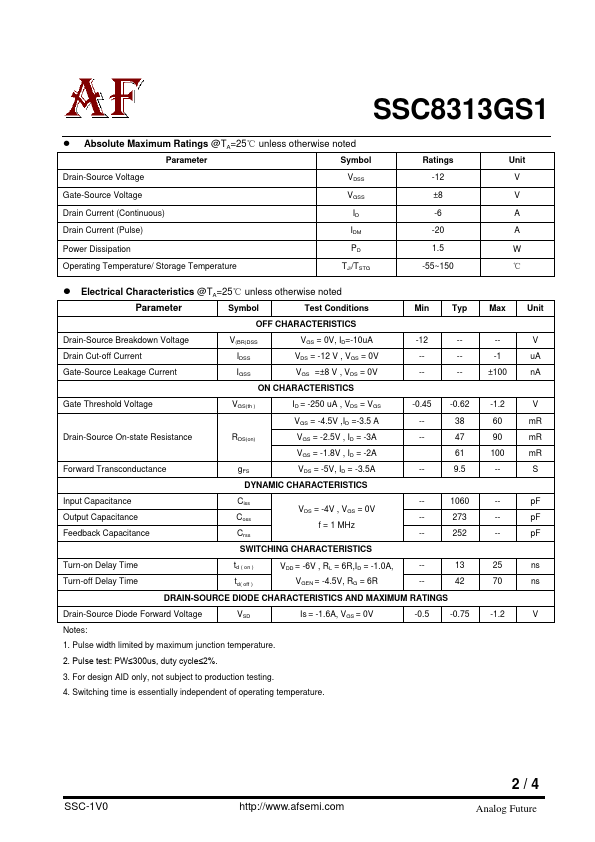
ABSOLUTE MAXIMUM RATINGS
@TA=25℃ unless otherwise noted Parameter Symbol Drain-Source Voltage VDSS Gate-Source Voltage