AK8443
AK8443 is 16bit 30MSPS video ADC manufactured by Asahi Kasei Microdevices.
[AK8443]
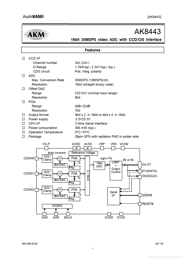
16bit 30MSPS video ADC with CCD/CIS interface Features
CCD I/F Channel number D-Range CDS circuit ADC Max. Conversion Rate Resolution Offset DAC Range Resolution PGA Range Resolution Output format Power supply CPU I/F Power consumption Operation Temperature: Package
VCLP
Black Correction
3ch (2ch.) 1.764Vpp / 2.341Vpp ( typ.) Pos. /Neg. polarity 30MSPS (10MSPS/ch) 16bit (straight binary code) ±321mV (normal input range) 8bit 0dB~22dB 7bit 8bit x 2 Æ 16bit or 4bit x 4 Æ 16bit 3.3V±0.3V 3 Wire Serial Interface 365 mW (typ.) 0°C~70°C 28pin QFN with radiation PAD in solder side
AVDD AVSS VRP VRN V
Reference Voltage PGA sign+17b 16bit ADC 3:1 MUX...