Am91L40
Am91L40 is 4096 x 1 Static R/W RAM manufactured by AMD.
- Part of the Am9140 comparator family.
- Part of the Am9140 comparator family.
DESCRIPTION
The Am9140 and Am91 L40 products are high performance, adaptive, low-power, 4k-bit, static, read/write random access memories. They are implemented as 4096 words by 1 bits per word. Only a single +5V power supply is required for normal operation. A DC power-down mode reduces power while retaining data with a supply voltage as low as 1.5V.
All interface signal levels are identical to TTL specifications, providing good noise immunity and simplified system design. All inputs are purely capacitive MOS loads. The outputs will drive two full TTL loads or more than eight low-power Schottky loads.
Operational cycles are initiated when the Chip Enable clock goes HIGH. When the read or write is plete, Chip Enable goes LOW to preset the memory for the next cycle. Address and Chip Select signals are latched on-chip to simplify system timing. Output data is also latched and is available until the next operating cycle. The WE signal is HIGH for all read operations and is LOW during the Chip Enable time to perform a write.
Memory Status is an output signal that indicates when data is actually valid and when the preset interval is plete. It can be used to generate the CE input and to improve the memory performance.
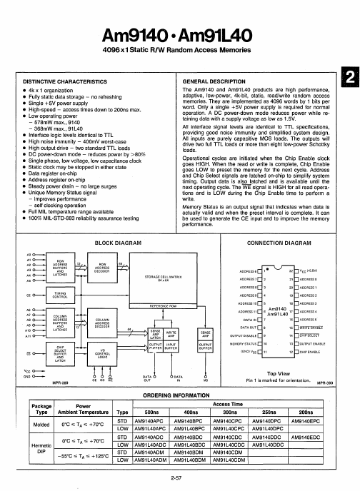
BLOCK DIAGRAM
CONNECTION DIAGRAM
AO Al A2 A3 A4 A5
A6 A7 A8 A9 Al0 All
VCC 0
- GND 0
- -
MPR- 389
ADDRESS
DECODER
COLUMN ADDRESS DECODER
1/0 CONTROL
LOGIC
STORAGE CELL MATRIX 64x64
,J OUT
SENSE AMP
OUTPUT BUFFER
DATA
ADDRESS 6 ADDRESS 7 ADDRESS 8 ADDRESS 9 ADDRESS 10 ADDRESS 11
DATA IN DATA OUT OUTPUT DISABLE MEMORY STATUS (GND) VSS
VCC (+5.0V) ADDRESS 0 ADDRESS 1 ADDRESS 2 ADDRESS 3 ADDRESS 4 ADDRESS 5 WRITE ENABLE CHIP SELECT OUTPUT ENABLE CHIP ENABLE
Top View
Pin 1 is marked for orientation.
MPR- 390
Package
Power
Type Ambient Temperature
Molded
O°C ,,;;; TA ,,;;; + 70°C
Hermetic DIP
O°C,,;;; TA ,,;;; +70°C -55°C,,;;; TA ,,;;;...