AN64 Overview
Key Specifications
Mount Type: Surface Mount
Pins: 64
Max Voltage (typical range): 5.5 V
Min Voltage (typical range): 2.7 V
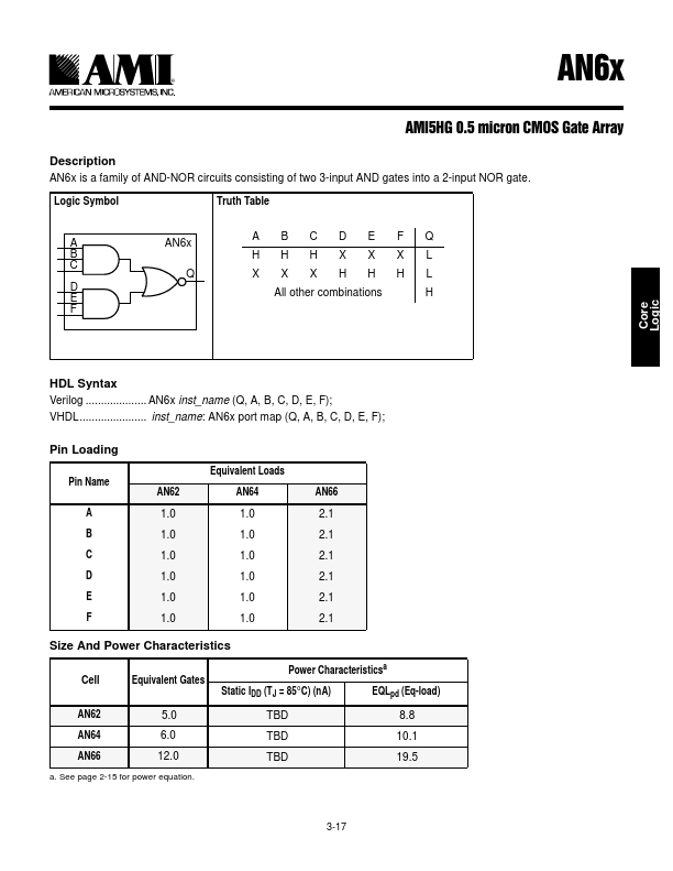
Description
AN6x is a family of AND-NOR circuits consisting of two 3-input AND gates into a 2-input NOR gate. Logic Symbol Truth Table A AN6x A BCDE FQ B HHHXXX L C Q XXXHHHL D E All other combinations H F Core Logic HDL Syntax Verilog.