IDQS3
IDQS3 is CMOS Gate Array manufactured by AMI.
,'46
®
$0,+- PLFURQ &026
- DWH $UUD
Description
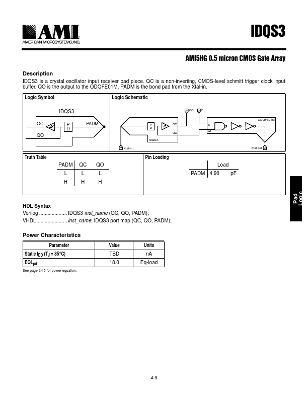
IDQS3 is a crystal oscillator input receiver pad piece. QC is a non-inverting, CMOS-level schmitt trigger clock input buffer. QO is the output to the ODQFE01M. PADM is the bond pad from the Xtal-in.
Logic Symbol
Logic Schematic
QC P PADM D
Truth Table
PADM L H
QC L H
QO L H
Xtal-in
QC E
QC E QI
Pin Loading
Load PADM 4.90 pF
ODQFE01M Xtal-out
HDL Syntax Verilog .................... IDQS3 inst_name (QC, QO, PADM); VHDL...................... inst_name: IDQS3 port map (QC, QO, PADM);
Power Characteristics
Parameter Static IDD (TJ = 85°C) EQLpd
See page 2-15 for power equation.
Value TBD 18.0
Units nA...