ODCSXE04
ODCSXE04 is CMOS Gate Array manufactured by AMI.
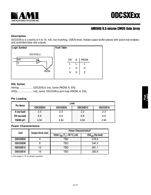
Description
ODCSXExx is a family of 4 to 16 m A, non-inverting, CMOS-level, tristate output buffer pieces with active low enables and controlled slew rate outputs.
Logic Symbol
Truth Table
ODCSXExx EN
PADM
EN A PADM
HDL Syntax Verilog ODCSXExx inst_name (PADM, A, EN); VHDL inst_name: ODCSXExx port map (PADM, A, EN);
Pin Loading
Pin Name
A (eq-load) EN (eq-load) PADM (p F)
ODCSXE04 2.3 6.9 4.94
Power Characteristics
Cell Output Drive (m A)
ODCSXE08
ODCSXE12
ODCSXE16
16 a. See page 2-15 for power equation.
ODCSXE08 2.3 6.9 4.94
Load
ODCSXE12 2.3 6.9 4.94
ODCSXE16 2.3 6.9 4.94
Power Characteristicsa
Static IDD (TJ = 85°C) (n A) TBD
EQLpd (Eq-load) 218.9
Pad Logic
4-17
2'&6;([[
®...