ODTSXX04
ODTSXX04 is CMOS Gate Array manufactured by AMI.
2'76;;[[
®
$0,+- PLFURQ &026
- DWH $UUD
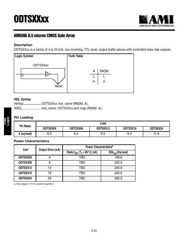
Description ODTSXXxx is a family of 4 to 24 m A, non-inverting, TTL-level, output buffer pieces with controlled slew rate outputs.
Logic Symbol
Truth Table
ODTSXXxx A SL
PADM
A PADM LL HH
HDL Syntax Verilog .................... ODTSXXxx inst_name (PADM, A); VHDL...................... inst_name: ODTSXXxx port map (PADM, A);
Pin Loading
Pin Name A (eq-load)
ODTSXX04 9.3
Power Characteristics
Cell Output Drive (m A)
ODTSXX08
ODTSXX12
ODTSXX16
ODTSXX24
24 a. See page 2-15 for power equation.
ODTSXX08 9.3
Load ODTSXX12
ODTSXX16 9.3
Power Characteristicsa
Static IDD (TJ = 85°C) (n A) TBD
EQLpd (Eq-load) 198.6
ODTSXX24 11.4
Pad...