FEATURES
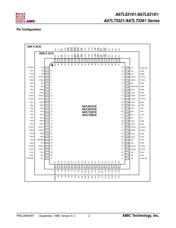
n Fast access time: 10/11/12 ns (100, 90, 83 MHz) n Direct Bus Alternation between READ and WRITE cycles allows 100% bus utilization n Signal +3.3V ± 5% power supply n Individual Byte Write control capability n Clock enable ( CEN ) pin to enable clock and suspend operations n Clock-controlled and registered address, data and control signals n Registered output for pipelined applications n Three separate chip enables allow wide range of options for CE control, address pipelining n Internally self-timed write cycle n Selectable BURST mode (Linear or Interleaved) n SLEEP mode (ZZ pin) provided n Available in 100 pin LQFP package LVTTL, Flow-through DBATM SRAM GENERAL DESCRIPTION
The AMIC Direct Bus Alternation™ (DBA™) SRAM family employs high-speed, low-power CMOS designs using an advanced CMOS process. The synchronous inputs include all address, all data inputs, active low chip enable ( CE ), two additional chip enables for easy depth expansion (CE2, CE2 ), cycle start input (ADV/LD ), synchronous clock enable ( CEN ), byte write enables ( BW1, BW2 , BW3 , BW4 ) and read/write (R/ W ). AMIC Technology