ASI MT5C1001
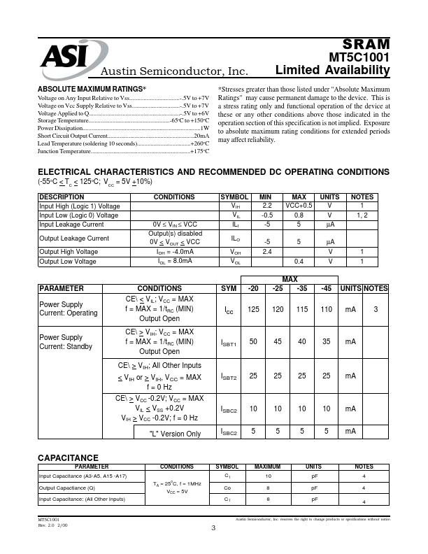
The MT5C1001 employs low power, high-performance silicon-gate CMOS technology. For flexibility in high-speed memory applications, ASI offers chip enable (CE\) and output enable (OE\) capability. These enhancements can place the outputs in High-Z for additional flexibility in system design.| Part No. | MT5C1001 |
|---|---|
| Datasheet | MT5C1001 Download |
| Manufacturer |  ASI |
| Description | SRAM |
| Buy | Stock & Price |
FEATURES
●●
●
●
●
●
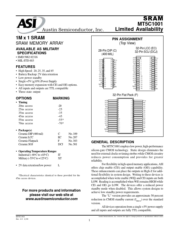
● High Speed: 20, 25, 35, and 45 Battery Backup: 2V data retention Low power standby Single +5V (+10%) Power Supply Easy memory expansion with CE\ and OE\ options. All inputs and outputs are TTL compatible Three-state output 32-Pin Flat Pack (F) OPTIONS
● Timing 20ns access 25ns access 35ns access 45ns access 55ns access 70ns access
● Package(s) Ceramic DIP (400 mil) Ceramic LCC Ceramic Flatpack Ceramic SOJ MARKING -20 -25 -35 -45 -55* -70* A10 A11 A12 NC A13 A14 A15 NC A16 A17 A18 A19 NC Q WE\ Vss 1 2 3 4 5 6 7 8 9 10 11 12 13 14 15 16 32 31 30 29 28 27 26 25 24 23 22 21 20 19 18 17 Vcc NC A9 A8 A7 A6 A5 A4 A3 NC A2 NC A1 A0 D CE\ C EC F DCJ No. 109 No. 207 No. 303 No. 501
GENERAL DESCRIPTION
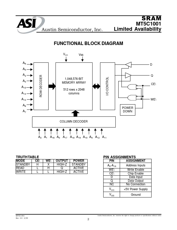
Static design eliminates the need for external clocks or timing strobes while CMOS circuitry reduces power consumption and provides for greater reliability. Writing to these devices is accomplished when write enable (WE|) and CE\ inputs are both LOW. Reading is accomplished when WE\ remains HIGH while CE\ and OE\ go LOW.