25F512AN Description
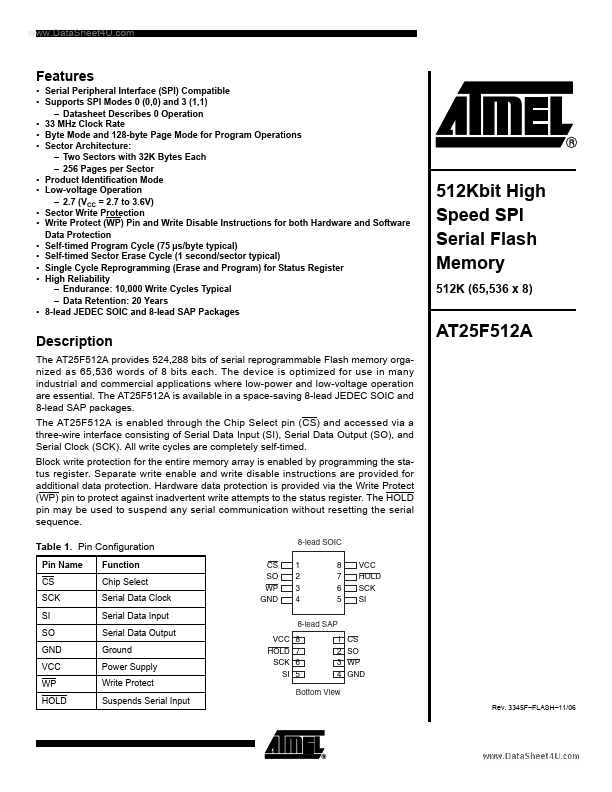
The AT25F512A provides 524,288 bits of serial reprogrammable Flash memory organized as 65,536 words of 8 bits each. The device is optimized for use in many industrial and mercial applications where low-power and low-voltage operation are essential. The AT25F512A is available in a space-saving 8-lead JEDEC SOIC and 8-lead SAP packages.
25F512AN Key Features
- Serial Peripheral Interface (SPI) patible
- Supports SPI Modes 0 (0,0) and 3 (1,1)
- Datasheet Describes 0 Operation
- 33 MHz Clock Rate
- Byte Mode and 128-byte Page Mode for Program Operations
- Sector Architecture
- Two Sectors with 32K Bytes Each
- 256 Pages per Sector Product Identification Mode Low-voltage Operation
- 2.7 (VCC = 2.7 to 3.6V) Sector Write Protection Write Protect (WP) Pin and Write Disable Instructions for both Hardware
- Endurance: 10,000 Write Cycles Typical