AMMC-5025
AMMC-5025 is TWA manufactured by Avago Technologies.
Description
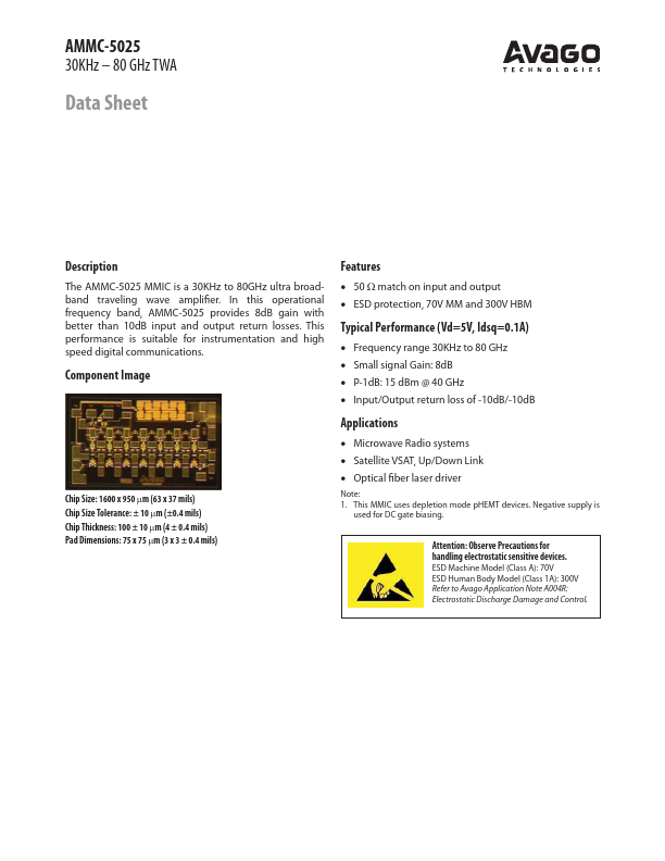
The AMMC-5025 MMIC is a 30KHz to 80GHz ultra broadband traveling wave amplifier. In this operational frequency band, AMMC-5025 provides 8d B gain with better than 10d B input and output return losses. This performance is suitable for instrumentation and high speed digital munications. ponent Image
Features x 50 : match on input and output x ESD protection, 70V MM and 300V HBM
Typical Performance (Vd=5V, Idsq=0.1A) x Frequency range 30KHz to 80 GHz x Small signal Gain: 8d B x P-1d B: 15 d Bm @ 40 GHz x Input/Output return loss of -10d B/-10d B
Chip Size: 1600 x 950 Pm (63 x 37 mils) Chip Size Tolerance: ± 10 Pm (±0.4 mils) Chip Thickness: 100 ± 10 Pm (4 ± 0.4 mils) Pad Dimensions: 75 x 75 Pm (3 x 3 ± 0.4 mils)
Applications x Microwave Radio systems x Satellite VSAT, Up/Down Link x Optical fiber laser driver
Note: 1. This MMIC uses depletion mode p HEMT devices. Negative supply is used for DC gate biasing.
Attention: Observe Precautions for handling electrostatic sensitive devices. ESD Machine Model (Class A): 70V ESD Human Body Model (Class 1A): 300V Refer to Avago Application Note A004R: Electrostatic Discharge Damage and Control.
Absolute Maximum Ratings[1,2,3, and 4]
Symbol
Parameters
Unit Max
Vd Positive Supply Voltage[2]
V7
Vg1 Gate Supply Voltage
V -3.6 to 0
Vg2 Gate Supply Voltage
V -2.5 to +2.5
PD Power Dissipation[2]
W 0.8
Pin CW Input Power d Bm 23
Tch Operating Channel Temp.
°C +150
Tstg Storage Case Temp.
°C -65 to +155
Tmax Maximum Assembly Temp (30 sec max) °C +320
Notes: 1. Operation in excess of any one of these conditions may result in permanent damage to this device. 2. binations of supply voltage and drain current shall not exceed PD. 3. The operating channel temperature will directly affect the device MTTF. For maximum life, it is remended that junction temperatures be maintained at the lowest possible levels.
DC Specifications/ Physical Properties [5]
Symbol Vd Id(q) Vg1 Vg2 RTjc Tch
Parameters and Test Conditions Drain...