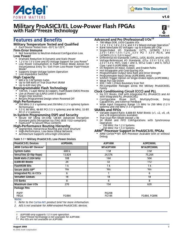
A3PE600L Overview
Key Specifications
Package: BGA
Mount Type: Surface Mount
Pins: 484
Operating Voltage: 1.5 V
Key Features
- Each Device Tested from –55°C to 125°C ® Advanced and Pro (Professional) I/Os††
- Not Susceptible to Neutron-Induced Configuration Loss Low Power
- Dramatic Reduction in Dynamic and Static Power
- 1.2 V to 1.5 V Core and I/O Voltage Support for Low Power†
- Low Power Consumption in Flash*Freeze Mode Allows for Instantaneous Entry To / Exit From Low-Power Flash*Freeze Modeƒ
- Supports Single-Voltage System Operation
- Low-Impedance Switches High Capacity
- 600 k to 3 M System Gates
- Up to 504 kbits of True Dual-Port SRAM
- Up to 620 User I/Os Reprogrammable Flash Technology

