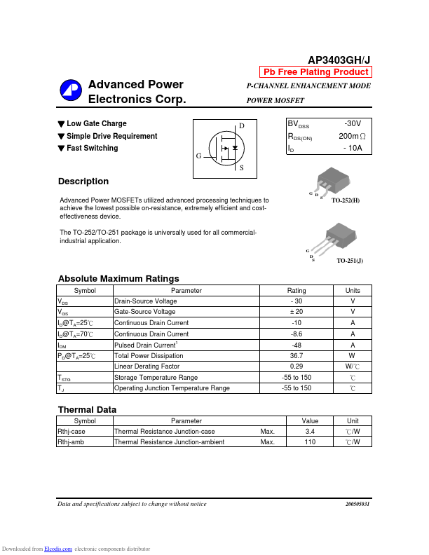
The following content is an automatically extracted verbatim text
from the original manufacturer datasheet and is provided for reference purposes only.
View original datasheet text
AP3403GH/J
Pb Free Plating Product
Advanced Power Electronics Corp.
▼ Low Gate Charge ▼ Simple Drive Requirement ▼ Fast Switching G S D
P-CHANNEL ENHANCEMENT MODE POWER MOSFET
BVDSS RDS(ON) ID
-30V 200mΩ - 10A
Description
G D
Advanced Power MOSFETs utilized advanced processing techniques to achieve the lowest possible on-resistance, extremely efficient and costeffectiveness device. The TO-252/TO-251 package is universally used for all commercialindustrial application.
G D S
S
TO-252(H)
TO-251(J)
Absolute Maximum Ratings
Symbol VDS VGS ID@TA=25℃ ID@TA=70℃ IDM PD@TA=25℃ TSTG TJ Parameter Drain-Source Voltage Gate-Source Voltage Continuous Drain Current Continuous Drain Current Pulsed Drain Current
1
Rating - 30 ± 20 -10 -8.6 -48 36.7 0.