AP60L02S
AP60L02S is N-CHANNEL ENHANCEMENT MODE POWER MOSFET manufactured by Advanced Power Electronics Corp.
- Part of the AP60L02P comparator family.
- Part of the AP60L02P comparator family.
Description
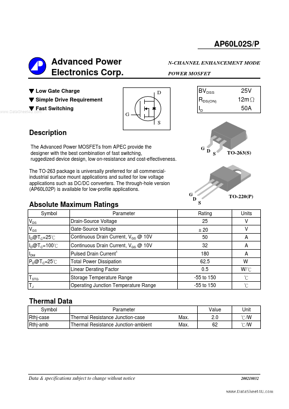
The Advanced Power MOSFETs from APEC provide the designer with the best bination of fast switching, ruggedized device design, low on-resistance and cost-effectiveness. The TO-263 package is universally preferred for all mercialindustrial surface mount applications and suited for low voltage applications such as DC/DC converters. The through-hole version (AP60L02P) is available for low-profile applications. G D G D S
TO-263(S)
TO-220(P)
S Rating 25 ± 20 50 32 180 62.5 0.5 Units V V A A A W W/ ℃ ℃ ℃
Absolute Maximum Ratings
Symbol VDS VGS ID@TC=25℃ ID@TC=100℃ IDM PD@TC=25℃ TSTG TJ Parameter Drain-Source Voltage Gate-Source Voltage Continuous Drain Current, VGS @ 10V Continuous Drain Current, VGS @ 10V Pulsed Drain Current
Total Power Dissipation Linear Derating Factor Storage Temperature Range Operating Junction Temperature Range
-55 to 150 -55 to 150
Thermal Data
Symbol Rthj-case Rthj-amb Parameter Thermal Resistance Junction-case Thermal Resistance Junction-ambient Max. Max. Value 2.0 62 Unit ℃/W ℃/W
Data & specifications subject to change without notice
AP60L02S/P
Electrical Characteristics@Tj=25o C(unless otherwise specified)
Symbol BVDSS
ΔBVDSS/ΔTj
Parameter Drain-Source Breakdown Voltage
Test Conditions VGS=0V, ID=250u A
Min. 25 1
- Typ. 0.037
Max. Units 12 26 3 1 25 ±100 V V/℃ mΩ mΩ V S u A u A n A n C n C n C ns ns ns ns p F p F p F
Breakdown Voltage Temperature Coefficient Reference to 25℃, ID=1m A
RDS(ON)
..
Static Drain-Source On-Resistance
VGS=10V, ID=25A VGS=4.5V, ID=20A
30 21 2.8 16 8 75 22 20 605 415 195
VGS(th) gfs IDSS IGSS Qg Qgs Qgd td(on) tr td(off) tf Ciss Coss Crss
Gate Threshold Voltage Forward Transconductance
Drain-Source Leakage Current (Tj=25 C) Drain-Source Leakage Current (Tj=150 C) o o
VDS=VGS, ID=250u A VDS=10V, ID=25A VDS=25V, VGS=0V VDS=20V, VGS=0V VGS= ± 20V ID=25A VDS=20V VGS=5V VDS=15V ID=20A RG=3.3Ω,VGS=10V RD=0.75Ω VGS=0V VDS=25V f=1.0MHz
Gate-Source Leakage Total Gate Charge
Gate-Source...