AP90T03GH
AP90T03GH is N-CHANNEL ENHANCEMENT MODE POWER MOSFET manufactured by Advanced Power Electronics Corp.
AP90T03GH/J
Pb Free Plating Product
Advanced Power Electronics Corp.
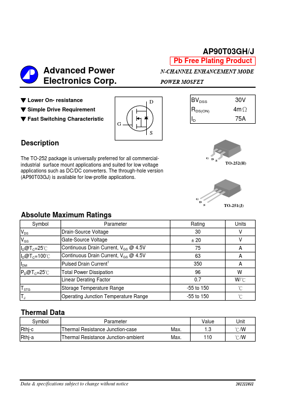
▼ Lower On- resistance ▼ Simple Drive Requirement ▼ Fast Switching Characteristic G S D
N-CHANNEL ENHANCEMENT MODE POWER MOSFET
BVDSS RDS(ON) ID
30V 4mΩ 75A
Description
The TO-252 package is universally preferred for all mercialindustrial surface mount applications and suited for low voltage applications such as DC/DC converters. The through-hole version (AP90T03GJ) is available for low-profile applications.
TO-252(H)
TO-251(J)...