Advanced Power Technology APL501J
N-Channel MOSFET
| Part No. | APL501J |
|---|---|
| Datasheet | APL501J Download |
| Manufacturer |  Advanced Power Technology |
| Description | N-Channel MOSFET |
| Buy | Stock & Price |
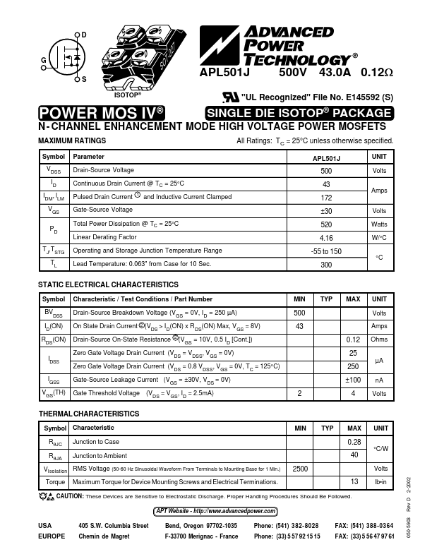
MAXIMUM RATINGS
All Ratings: TC = 25°C unless otherwise specified. Symbol Parameter VDSS ID IDM, lLM VGS Drain-Source Voltage Continuous Drain Current @ TC = 25°C Pulsed Drain Current 1 and Inductive Current Clamped Gate-Source Voltage PD Total Power Dissipation @ TC = 25°C Linear Derating Factor TJ,TSTG TL Operating and Storage Junction Temperature Range Lead Temperature: 0.063" from Case for 10 Sec. APL501J 500 43 172 ±30 520 4.16 -55 to 150 300 UNIT Volts Amps Volts Watts W/°C °C STATICELECTRICAL CHARACTERISTICS
Symbol Characteristic / Test Conditions / Part Number MIN TYP MAX UNIT BVDSS Drain-Source Breakdown Voltage (VGS = 0V, ID = 250 µA) 500 ID(ON) On State Drain Current 2 (VDS > ID(ON) x RDS(ON) Max, VGS = 8V) 43 RDS(ON) Drain-Source On-State Resistance 2 (VGS = 10V, 0.5 ID [Cont.]) IDSS Zero Gate Voltage Drain Current (VDS = VDSS, VGS = 0V) Zero Gate Voltage Drain Current (VDS = 0.8 VDSS, VGS = 0V, TC = 125°C) IGSS Gate-Source Leakage Current (VGS = ±30V, VDS = 0V) VGS(TH) Ga...