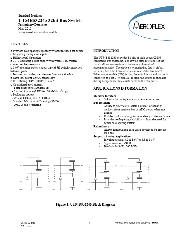
UT54BS32245 Overview
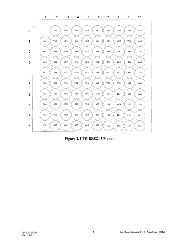
Pin No. A2, A3, A4, A5, A6, A7, A8, A9, B1, B10, C1, C10, D1, D10, E1, E10, F1, F10, G1, G10, H1, H10, J1, J10, K2, K3, K4, K5, K6, K7, K8, K9 B3, B4, B5, B6, B7, B8, C2, C4, C7, C9, D2, D3, D8, D9, E2, E9, F2, F9, G2, G3, G8, G9, H2, H4, H7, H9, J3, J4, J5,.
UT54BS32245 Key Features
- Provides cold-sparing capability without the need for actual cold-sparing multiplexer inputs
- Bidirectional Operation
- 3.3 V operating power supply with typical 11Ω switch connection between ports
- 5.0V operating power supply typical 5Ω switch connection between ports
- Isolates non cold-spared devices from an active bus
- Ultra low power CMOS technology
- ESD Rating HBM: 2000V, Class 2
- Operational environment
- Total-dose: up to 300 krad(Si)
- Latchup immune (LET <= 100 MeV-cm2/mg)
UT54BS32245 Applications
- Solution for multiple memory devices on a bus
- Ability to electrically isolate a device, or banks of devices, from memory bus or ADC output when not needed
- Enables bank switching for redundancy or device failure
- Provides cold-sparing capability without the need for actual cold-sparing buffers
- Allows multiple non cold-spare devices to be present on a bus
- In voltage range: 3.0 to 3.6V or 4.5 to 5.5V