FEATURES
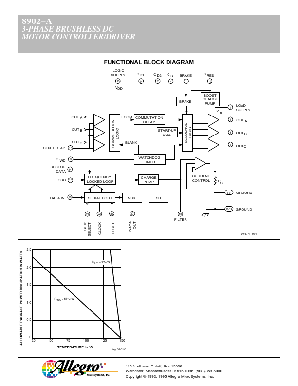
s s s s s s s s s s s s s s s s s DMOS Outputs Low rDS(on) Startup Commutation Circuitry Back-EMF Commutation Circuitry Serial Port Interface Frequency-Locked Loop Speed Control Sector Data Tachometer Signal Input Programmable Start-Up Current Diagnostics Mode Sleep Mode Linear Current Control Internal Current Sensing Dynamic Braking Through Serial Port Power-Down Dynamic Braking System Diagnostics Data Out Data Out Ported in Real Time Internal Thermal Shutdown Circuitry ABSOLUTE MAXIMUM RATINGS
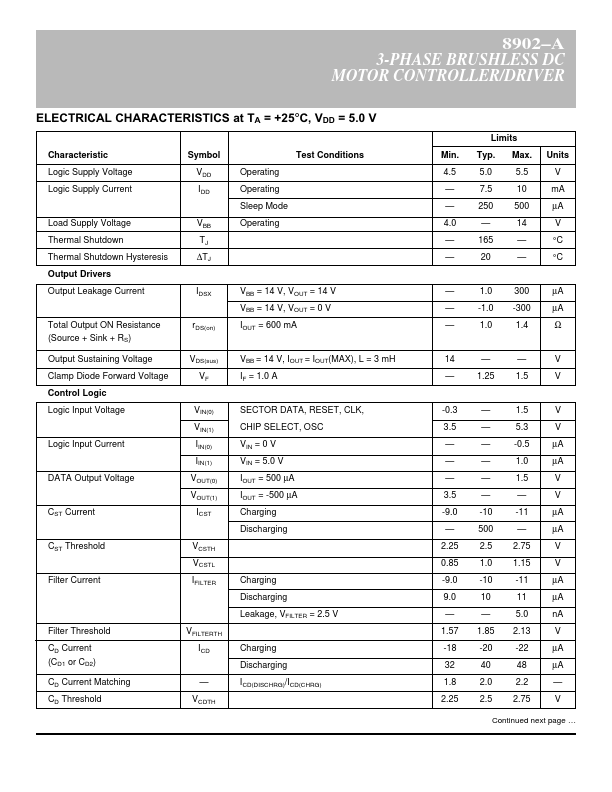
at TA = +25°C Load Supply Voltage, VBB . . . . . . . . . . 14 V Output Current, IOUT . . . . . . . . . . . . ±1.25 A Logic Supply Voltage, VDD . . . . . . . . . 6.0 V Logic Input Voltage Range, VIN . . . . . . . . . . . -0.3 V to VDD + 0.3 V Package Power Dissipation, PD See Graph Operating Temperature Range, TA . . . . . . . . . . . . . . . . . . 0°C to +70°C Junction Temperature, TJ . . . . . . . +150°C† Storage Temperature Range, TS . . . . . . . . . . . . . . . -55°C to +150°C † Fault conditions that produce excessive junction temperature will activate device thermal shutdown circuitry. Allegro MicroSystems