AS7C33128NTD18B Overview
Key Features
- Organization: 131,072 words × 18 bits
- NTD™ architecture for efficient bus operation
- Fast clock speeds to 200 MHz
- Fast clock to data access: 3.0/3.5/4.0 ns
- Fast OE access time: 3.0/3.5/4.0 ns
- Fully synchronous operation
- Asynchronous output enable control
- Available in 100-pin TQFP package
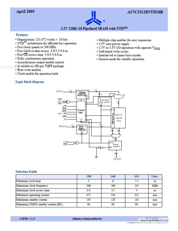
- Clock enable for operation hold Logic A[16:0] 17 D
- Multiple chip enables for easy expansion