AS7C3364PFS32A
AS7C3364PFS32A is 3.3V 64K X 32/36 pipeline burst synchronous SRAM manufactured by Alliance Semiconductor Corporation.
Features
- Organization: 65,536 words × 32 or 36 bits
- Fast clock speeds to 166 MHz in LVTTL/LVCMOS
- Fast clock to data access: 3.5/3.8/4.0/5.0 ns
- Fast OE access time: 3.5/3.8/4.0/5.0 ns
- Fully synchronous register-to-register operation
- Single register “Flow-through” mode
- Single-cycle deselect
- Pentium®- patible architecture and timing
..
- Asynchronous output enable control
- Economical 100-pin TQFP package
- Byte write enables
- Multiple chip enables for easy expansion
- 3.3 core power supply
- 2.5V or 3.3V I/O operation with separate VDDQ
- 30 m W typical standby power in power down mode
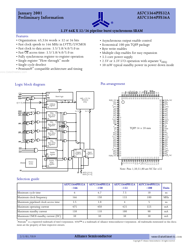
Logic block diagram
LBO CLK ADV ADSC ADSP A[15:0] 16 CLK CE CLR D CE Address register CLK D Q0 Burst logic Q1 16 Q
Pin arrangement
A6 A7 CE0 CE1 BWd BWc BWb BWa CE2 VDD VSS CLK GWE BWE OE ADSC ADSP ADV A8 A9 64K × 32/36 Memory array 100 99 98 97 96 95 94 93 92 91 90 89 88 87 86 85 84 83 82 81
GWE BWE BWd
DQd Q Byte write registers CLK D DQc Q Byte write registers CLK D DQb Q Byte write registers CLK D DQa Q Byte write registers CLK D Enable CE register CLK Power down D Enable Q delay register CLK Q
36/32
36/32
BWc
BWb
BWa CE0 CE1 CE2
OE FT DATA [35:0] DATA [31:0]
Note: Pins 1,30,51,80 are NC for ×32
Selection guide
- 166 Minimum cycle time Maximum clock frequency Maximum pipelined clock access time Maximum operating current Maximum standby current Maximum CMOS standby current (DC)
- ®
- 150 6.7 150 3.8 450 110 30
- 133 7.5 133 4 425 100 30
LBO A5 A4 A3 A2 A1 A0 NC NC VSS VDD NC NC A10 A11 A12 A13 A14 A15 NC
31 32 33 34 35 36 37 38 39 40 41 42 43 44 45 46 47 48 49...