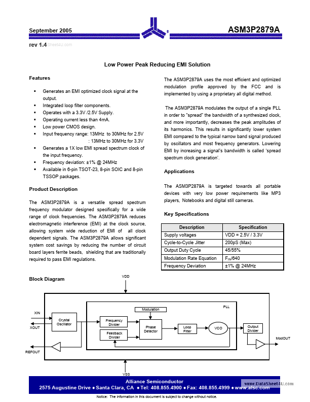
ASM3P2879A Overview
Description
Supply voltages Cycle-to-Cycle Jitter Output Duty Cycle Modulation Rate Equation Frequency Deviation Specification VDD = 2.5V / 3.3V 200pS (Max) 45/55% FIN/640 ±1% @ 24MHz VDD.
Key Features
- Generates an EMI optimized clock signal at the output
- Integrated loop filter components
- Operates with a 3.3V /2.5V Supply
- Operating current less than 4mA
- Low power CMOS design
- Input frequency range: 13MHz to 30MHz for 2.5V : 13MHz to 30MHz for 3.3V Generates a 1X low EMI spread spectrum clock of the input frequency
- Frequency deviation: ±1% @ 24MHz Available in 6-pin TSOT-23, 8-pin SOIC and 8-pin TSSOP packages
- Lowering EMI by increasing a signal’s bandwidth is called ‘spread spectrum clock generation’