AO3407
Description
The AO3407 uses advanced trench technology to provide excellent RDS(ON) with low gate charge. This device is suitable for use as a load switch or in PWM applications.
Product Summary
VDS ID (at VGS= -10V) RDS(ON) (at VGS= -10V) RDS(ON) (at VGS = -4.5V)
-30V -4.1A < 52m W < 87m W
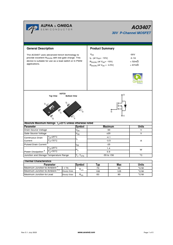
SOT23
Top View
Bottom View
Absolute Maximum Ratings TA=25°C unless otherwise noted
Parameter
Symbol
Drain-Source Voltage
Gate-Source Voltage
Continuous Drain Current
TA=25°C TA=70°C
Pulsed Drain Current C
TA=25°C Power Dissipation B TA=70°C
Junction and Storage Temperature Range
TJ, TSTG
Maximum -30 ±20 -4.1 -3.5 -25 1.4 0.9
-55 to 150
Thermal Characteristics
Parameter
Symbol
Typ
Maximum Junction-to-Ambient A t ≤ 10s Maximum Junction-to-Ambient A D Steady-State
Rq JA
70 100
Maximum Junction-to-Lead
Steady-State
Rq JL
Max 90 125...