Datasheet Details
| Part number | AO3422 |
|---|---|
| Manufacturer | Alpha & Omega Semiconductors |
| File Size | 348.69 KB |
| Description | N-Channel MOSFET |
| Datasheet |
 AO3422 Datasheet AO3422 Datasheet
|
|
|
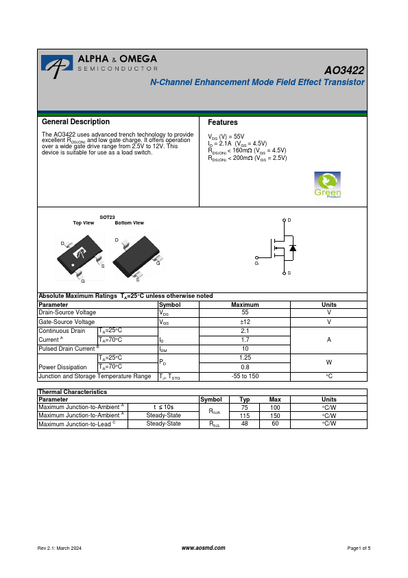
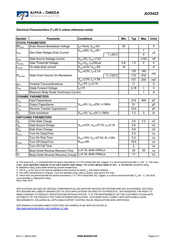
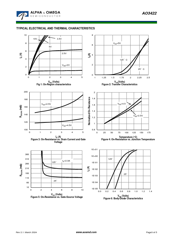
The AO3422 uses advanced trench technology to provide excellent RDS(ON) and low gate charge.
It offers operation over a wide gate drive range from 2.5V to 12V.
This device is suitable for use as a load switch.
| Part number | AO3422 |
|---|---|
| Manufacturer | Alpha & Omega Semiconductors |
| File Size | 348.69 KB |
| Description | N-Channel MOSFET |
| Datasheet |
AO3422 Datasheet
|
|
|
|
| Part Number | Description | Manufacturer |
|---|---|---|
| AO3422 | N-Channel MOSFET | Kexin |
| AO3420 | N-CHANNEL MOSFET | BLUE ROCKET ELECTRONICS |
| AO3420 | 20V N-Channel MOSFET | Oucan Semi |
| AO3420 | N-Channel MOSFET | Kexin |
| AO3421 | P-Channel MOSFET | Kexin |
| Part Number | Description |
|---|---|
| AO3420 | N-Channel MOSFET |
| AO3421 | 30V P-Channel MOSFET |
| AO3421E | 30V P-Channel MOSFET |
| AO3423 | 20V P-Channel MOSFET |
| AO3424 | 30V N-Channel MOSFET |
The following content is an automatically extracted verbatim text from the original manufacturer datasheet and is provided for reference purposes only.