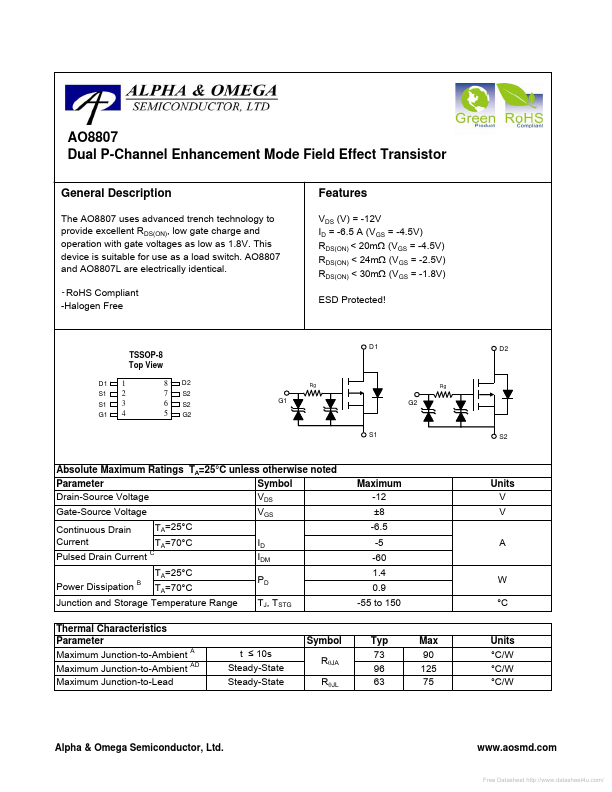
Datasheet4U Logo Datasheet4U.com

AO8807 - Dual P-Channel FET

General Description

The AO8807 uses advanced trench technology to provide excellent RDS(ON), low gate charge and operation with gate voltages as low as 1.8V.

This device is suitable for use as a load switch.

AO8807 and AO8807L are electrically identical.

Key Features

  • VDS (V) = -12V ID = -6.5 A (VGS = -4.5V) RDS(ON) < 20mΩ (VGS = -4.5V) RDS(ON) < 24mΩ (VGS = -2.5V) RDS(ON) < 30mΩ (VGS = -1.8V) ESD Protected! D1 TSSOP-8 Top View D1 S1 S1 G1 1 2 3 4 8 7 6 5 D2 S2 S2 G2 Rg Rg D2 G1 G2 S1 S2 Absolute Maximum Ratings TA=25°C unless otherwise noted Symbol Parameter VDS Drain-Source Voltage VGS Gate-Source Voltage Continuous Drain Current Pulsed Drain Current Power Dissipation B C Maximum -12 ±8 -6.5 -5 -60 1.4 0.9 -55 to 150 Units V V A TA=25°C TA=70°C TA.

📥 Download Datasheet

Full PDF Text Transcription (Reference)

The following content is an automatically extracted verbatim text from the original manufacturer datasheet and is provided for reference purposes only.

View original datasheet text
AO8807 Dual P-Channel Enhancement Mode Field Effect Transistor General Description The AO8807 uses advanced trench technology to provide excellent RDS(ON), low gate charge and operation with gate voltages as low as 1.8V. This device is suitable for use as a load switch. AO8807 and AO8807L are electrically identical. - RoHS Compliant -Halogen Free Features VDS (V) = -12V ID = -6.5 A (VGS = -4.5V) RDS(ON) < 20mΩ (VGS = -4.5V) RDS(ON) < 24mΩ (VGS = -2.5V) RDS(ON) < 30mΩ (VGS = -1.8V) ESD Protected! D1 TSSOP-8 Top View D1 S1 S1 G1 1 2 3 4 8 7 6 5 D2 S2 S2 G2 Rg Rg D2 G1 G2 S1 S2 Absolute Maximum Ratings TA=25°C unless otherwise noted Symbol Parameter VDS Drain-Source Voltage VGS Gate-Source Voltage Continuous Drain Current Pulsed Drain Current Power Dissipation B C Maximum -12 ±8 -6.