Datasheet Details
| Part number | AOWF190A60C |
|---|---|
| Manufacturer | Alpha & Omega Semiconductors |
| File Size | 464.80 KB |
| Description | N-Channel Power Transistor |
| Datasheet |
 AOWF190A60C Datasheet AOWF190A60C Datasheet
|
|
|
| Part number | AOWF190A60C |
|---|---|
| Manufacturer | Alpha & Omega Semiconductors |
| File Size | 464.80 KB |
| Description | N-Channel Power Transistor |
| Datasheet |
AOWF190A60C Datasheet
|
|
|
|
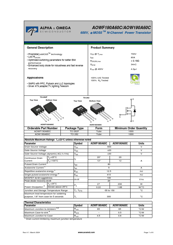
• Proprietary aMOS5TM technology • Low RDS(ON) • Optimized switching parameters for better EMI performance • Enhanced body diode for robustness and fast reverse recovery Applications • SMPS with PFC, Flyback and LLC topologies • Silver ATX,adapter,TV,lighting,Telecom Product Summary VDS @ Tj,max IDM RDS(ON),max Qg,typ Eoss @ 400V 100% UIS Tested 100% Rg Tested TO-262F Top View Bottom View TO-262 Top View Bottom View 700V 80A < 0.19Ω 34nC 4.3mJ D G DS G D S AOWF190A60C Orderable Part Number AOWF190A60C AOW190A60C Package Type TO-262F TO-262 S D G AOW190A60C Form Tube Tube G G SD S Minimum Order Quantity 1000 1000 Absolute Maximum Ratings TA=25°C unless otherwise noted Parameter Symbol AOWF190A60C AOW190A60C Drain-Source Voltage VDS 600 Gate-Source Voltage VGS ±20 Gate-Source Voltage (dynamic) AC( f>1Hz) Continuous Drain TC=25°C Current TC=100°C Pulsed Drain Current C Avalanche Current C Repetitive avalanche energy C Single pulsed avalanche energy G MOSFET dv/dt ruggedness Peak diode recovery dv/dt VGS ID IDM IAR EAR EAS dv/dt ±30 20* 20 12* 12 80 5 12.5 410 100 20 TC=25°C Power Dissipation B Derate above 25°C PD 27 208 0.22 1.66 Junction and Storage Temperature Range Maximum lead temperature for soldering purpose, 1/8" from case for 5 seconds TJ, TSTG TL -55 to 150 300 Units V V V A A mJ mJ V/ns W W/°C °C °C Thermal Characteristics Parameter Maximum Junction-to-Ambient A,D Maximum Case-to-sink A Symbol RqJA RqCS Maximum Junction-to-Case RqJC * Drain current limited by maximum junction temperature AOWF190A60C 65 -4.5 AOW190A60C 65 0.5 0.6 Units °C/W °C/W °C/W Rev.4.1: March 2024 www.aosmd.com Page 1 of 6 AOWF190A60C/AOW190A60C Electrical Characteristics (TJ=25°C unless otherwise noted) Symbol Parameter Conditions Min Typ Max Units STATIC PARAMETERS BVDSS Drain-Source Breakdown Voltage ID=250μA, VGS=0V, TJ=
AOWF190A60C/AOW190A60C 600V, a MOS5 TM N-Channel Power Transistor.
| Part Number | Description |
|---|---|
| AOWF190A60 | 600V N-Channel Power Transistor |
| AOWF10N60 | 10A N-Channel MOSFET |
| AOWF10N65 | 10A N-Channel MOSFET |
| AOWF10T60 | 10A N-Channel MOSFET |
| AOWF11C60 | 11A N-Channel MOSFET |
| AOWF11S60 | Power Transistor |
| AOWF11S65 | Power Transistor |
| AOWF125A60 | N-Channel Power Transistor |
| AOWF12N50 | 12A N-Channel MOSFET |
| AOWF12N60 | 12A N-Channel MOSFET |