AON3414 Overview
Key Specifications
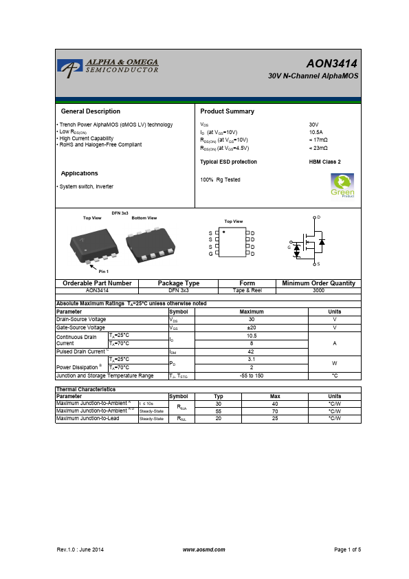
Package: SMD/SMT
Mount Type: Surface Mount
Max Operating Temp: 150 °C
Min Operating Temp: -55 °C
Description
Trench Power AlphaMOS (αMOS LV) technology - Low RDS(ON) - High Current Capability - RoHS and Halogen-Free Compliant.