AON7210 Overview
Description
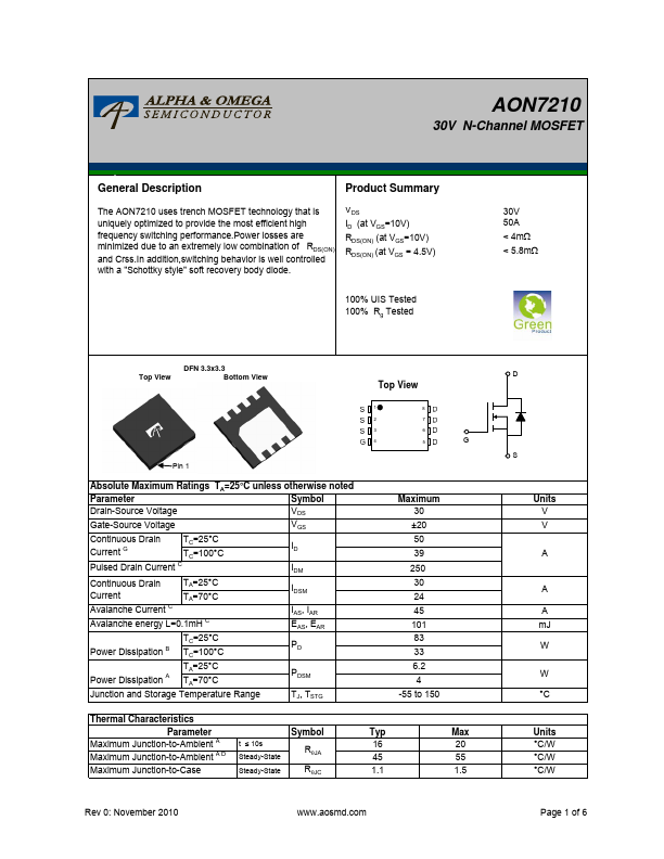
Product Summary The AON7210 uses trench MOSFET technology that is uniquely optimized to provide the most efficient high frequency switching losses are minimized due to an extremely low combination of RDS(ON) and addition,switching behavior is well controlled with a "Schottky style" soft recovery body diode. VDS ID (at VGS=10V) RDS(ON) (at VGS=10V) RDS(ON) (at VGS = 4.5V) 100% UIS Tested 100% Rg Tested 30V 50A < 4mΩ < 5.8mΩ DFN 3.3x3.3 Top View Bottom View Top View 18 27 36 4 5G Pin 1 Parameter Symbol Drain-Source Voltage VDS Gate-Source Voltage VGS Continuous Drain TC=25°C Current G TC=100°C Pulsed Drain Current C ID IDM Continuous Drain TA=25°C Current TA=70°C Avalanche Current C Avalanche energy L=0.1mH C IDSM IAS, IAR EAS, EAR TC=25°C Power Dissipation B TC=100°C PD TA=25°C Power Dissipation A TA=70°C PDSM Junction and Storage Temperature Range TJ, TSTG Maximum 30 ±20 50 39 250 30 24 45 101 83 33 6.2 4 -55 to 150 Parameter Maximum Junction-to-Ambient A Maximum Junction-to-Ambient A D Maximum Junction-to-Case t ≤ 10s Steady-State Steady-State Symbol RθJA RθJC Typ 16 45 1.1 Max 20 55 1.5 Rev 0: November 2010 D S Units V V A A A mJ W W °C Units °C/W °C/W °C/W Page 1 of 6 AON7210 Symbol Parameter Conditions Min Typ Max Units STATIC PARAMETERS BVDSS Drain-Source Breakdown Voltage ID=250µA, VGS=0V 30 V IDSS Zero Gate Voltage Drain Current VDS=30V, VGS=0V TJ=55°C 1 5 µA IGSS Gate-Body leakage current VDS=0V, VGS= ±20V 100 nA VGS(th) Gate Threshold Voltage VDS=VGS ID=250µA 1.3 1.8 2.3 V ID(ON) On state drain current VGS=10V, VDS=5V 250 A RDS(ON) Static Drain-Source On-Resistance VGS=10V, ID=20A TJ=125°C 3 4.7 4 6.2 mΩ VGS=4.5V, ID=20A.