AOSS21115C Overview
Key Specifications
Max Operating Temp: 150 °C
Min Operating Temp: -55 °C
Description
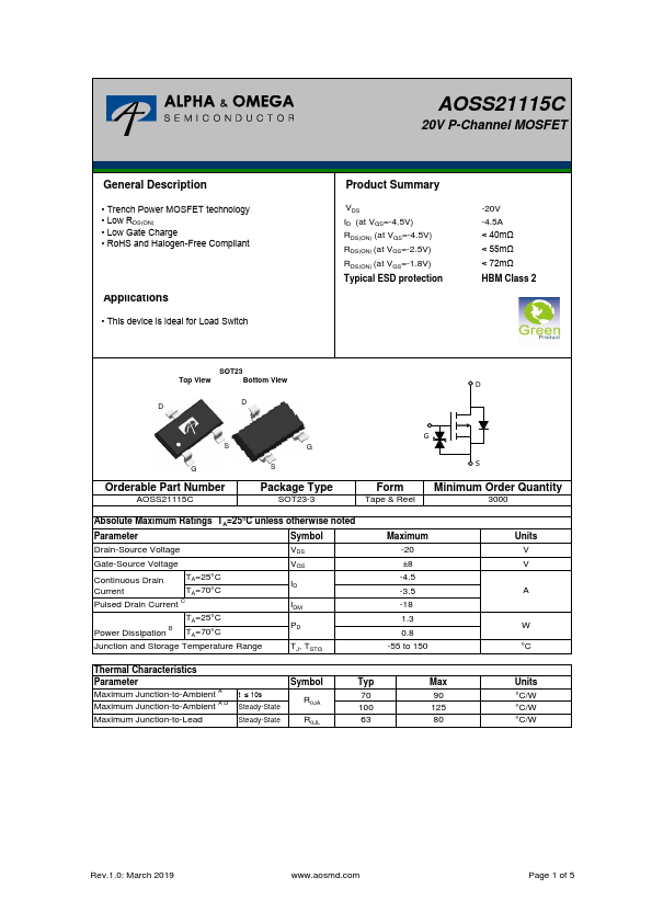
Trench Power MOSFET technology - Low RDS(ON) - Low Gate Charge - RoHS and Halogen-Free Compliant.
| Part | AOSS21115C |
|---|---|
| Description | 20V P-Channel MOSFET |
| Category | MOSFET |
| Manufacturer | Alpha & Omega Semiconductors |
| Size | 291.10 KB |
Max Operating Temp: 150 °C
Min Operating Temp: -55 °C
Trench Power MOSFET technology - Low RDS(ON) - Low Gate Charge - RoHS and Halogen-Free Compliant.
| Seller | Inventory | Price Breaks | Buy |
|---|---|---|---|
| DigiKey | 17853 | 1+ : 0.56 USD 10+ : 0.342 USD 100+ : 0.2171 USD 500+ : 0.16312 USD |
View Offer |
| DigiKey | 17853 | 1+ : 0.56 USD 10+ : 0.342 USD 100+ : 0.2171 USD 500+ : 0.16312 USD |
View Offer |
| Part Number | Manufacturer | Description |
|---|---|---|
| A2SHB | HAOHAI | N-Channel MOSFET |
| AP9563GH | Advanced Power Electronics Corp | P-CHANNEL ENHANCEMENT MODE POWER MOSFET |
| FCPF360N65S3R0L | onsemi | N-Channel MOSFET |