AOT12N50 Overview
Key Specifications
Package: TO-220
Mount Type: Through Hole
Max Operating Temp: 150 °C
Min Operating Temp: -55 °C
Description
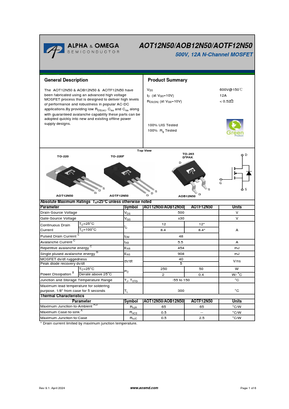
Product Summary The AOT12N50 & AOB12N50 & AOTF12N50 have been fabricated using an advanced high voltage MOSFET process that is designed to deliver high levels of performance and robustness in popular AC-DC providing low RDS(on), Ciss and Crss along with guaranteed avalanche capability these parts can be adopted quickly into new and existing offline power supply designs. VDS ID (at VGS=10V) RDS(ON) (at VGS=10V) 100% UIS Tested 100% Rg Tested TO-220 TO-220F Top View TO-263 D2PAK D 600V@150℃ 12A < 0.52W D G AOT12N50 DS G AOTF12N50 G DS S AOB12N50 G Parameter Symbol AOT12N50/AOB12N50 Drain-Source Voltage VDS 500 Gate-Source Voltage VGS ±30 Continuous Drain Current TC=25°C TC=100°C ID 12 8.4 Pulsed Drain Current C IDM 48 Avalanche Current C IAR 5.5 Repetitive avalanche energy C EAR 454 Single plused avalanche energy G EAS 908 MOSFET dv/dt ruggedness Peak diode recovery dv/dt dv/dt 40 5 TC=25°C Power Dissipation B Derate above 25oC PD 250 2 AOTF12N50 12* 8.4* 50 0.4 Junction and Storage Temperature Range Maximum lead temperature for soldering purpose, 1/8" from case for 5 seconds TJ, TSTG TL -55 to 150 300 Parameter Maximum Junction-to-Ambient A,D Maximum Case-to-sink A Symbol RqJA RqCS Maximum Junction-to-Case RqJC * Drain current limited by maximum junction temperature.