AOT12N50 Overview
Key Specifications
Package: TO-220
Mount Type: Through Hole
Max Operating Temp: 150 °C
Min Operating Temp: -55 °C
Description
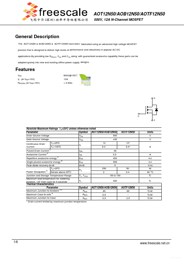
The AOT12N50 & AOB12N50 & AOTF12N50 have been fabricated using an advanced high voltage MOSFET process that is designed to deliver high levels of performance and robustness in popular AC-DC providing low RDS(on), Ciss and Crss along with guaranteed avalanche capability these parts can be adopted quickly into new and existing offline power supply designs.