AO7407 Overview
Key Specifications
Mount Type: Surface Mount
Max Operating Temp: 150 °C
Min Operating Temp: -55 °C
Description
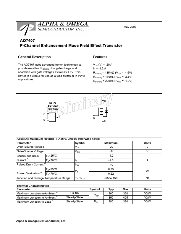
The AO7407 uses advanced trench technology to provide excellent RDS(ON), low gate charge and operation with gate voltages as low as 1.8V. This device is suitable for use as a load switch or in PWM applications.