FEATURES
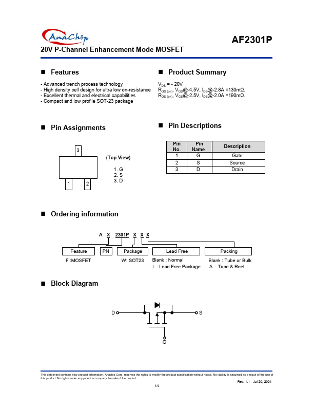
Product Summary - Advanced trench process technology - High density cell design for ultra low on-resistance - Excellent thermal and electrical capabilities - Compact and low profile SOT-23 package VDS = - 20V RDS (on), VGS@-4.5V, IDS@-2.8A =130mΩ. RDS (on), VGS@-2.5V, IDS@-2.0A =190mΩ. Pin Assignments 3 12 (Top View) 1. G 2. S 3. D Pin Descriptions Pin Pin No. Name 1G 2S 3D DESCRIPTION
Gate Source Drain Ordering information A X 2301P X X X Feature PN Package Lead Free Packing F :MOSFET W: SOT23 Blank : Normal Blank : Tube or Bulk L : Lead Free Package A : Tape & Reel Block Diagram DS G This datasheet contains new product information. Anachip Corp. reserves the rights to modify the product specification without notice. No liability is assumed as a result of the use of this product. No rights under any patent accompany the sale of the product. Rev. 1.1 Jul 20, 2004 1/4 20V P-Channel Enhancement Mode MOSF Anachip