AF4920N
AF4920N is N-Channel Enhancement Mode Power MOSFET manufactured by Anachip.
Features
- Low On-resistance
- Simple Drive Requirement
- Dual N MOSFET Package
- General Description
The advanced power MOSFET provides the designer with the best bination of fast switching, ruggedized device design, ultra low on-resistance and cost-effectiveness.
- Product Summary
BVDSS (V) 30 RDS(ON) (mΩ) 18 ID (A) 8.2
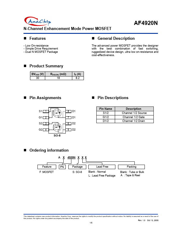
- Pin Assignments
- Pin Descriptions
Pin Name S1/2 G1/2 D1/2 Description
Channel 1/2 Source Channel 1/2 Gate Channel 1/2 Drain
S1 G1 S2 G2
1 2 3 4
8 7 6 5
D1 D1 D2 D2
SO-8
- Ordering information
A X Feature
F :MOSFET PN 4920N X X X Package S: SO-8 Lead Free Blank : Normal L : Lead Free Package Packing Blank : Tube or Bulk A : Tape & Reel
This datasheet contains new product information. Anachip Corp. reserves the rights to modify the product specification without notice. No liability is assumed as a result of the use of this product. No rights under any patent acpany the sale of the product.
Rev. 1.0 Oct 13, 2005 1/5
N-Channel Enhancement Mode Power MOSFET
- Absolute Maximum Ratings
Symbol VDS VGS ID IDM PD TSTG TJ Parameter Drain-Source Voltage Gate-Source Voltage Continuous Drain Current (Note 1) Pulsed Drain Current (Note 2) Total Power Dissipation Linear Derating Factor Storage Temperature Range Operating Junction Temperature Range TA=25ºC TA=70ºC TA=25ºC Rating 30 ±20 8.2 6.7 30 2 0.016 -55 to 150 -55 to 150 Units V V A A W W/ºC ºC ºC
- Thermal Data
Symbol Rthj-amb Parameter Thermal Resistance Junction-ambient (Note 1) Max. Maximum 62.5 Units ºC/W
- Electrical Characteristics at TJ=25ºC unless otherwise specified
Symbol BVDSS ∆BVDSS / ∆TJ RDS(ON) VGS(th) gfs IDSS IGSS Qg Qgs Qgd td(on) tr td(off) tf Ciss Coss Crss RG Parameter Drain-Source Breakdown Voltage Breakdown Voltage Temperature Coefficient Static Drain-Source On-Resistance (Note 3) Gate Threshold Voltage Forward Transconductance Drain-Source Leakage Current (TJ=25o C) Drain-Source Leakage Current (TJ=70o C) Gate-Source Leakage Total Gate Charge (Note 3)...