FEATURES
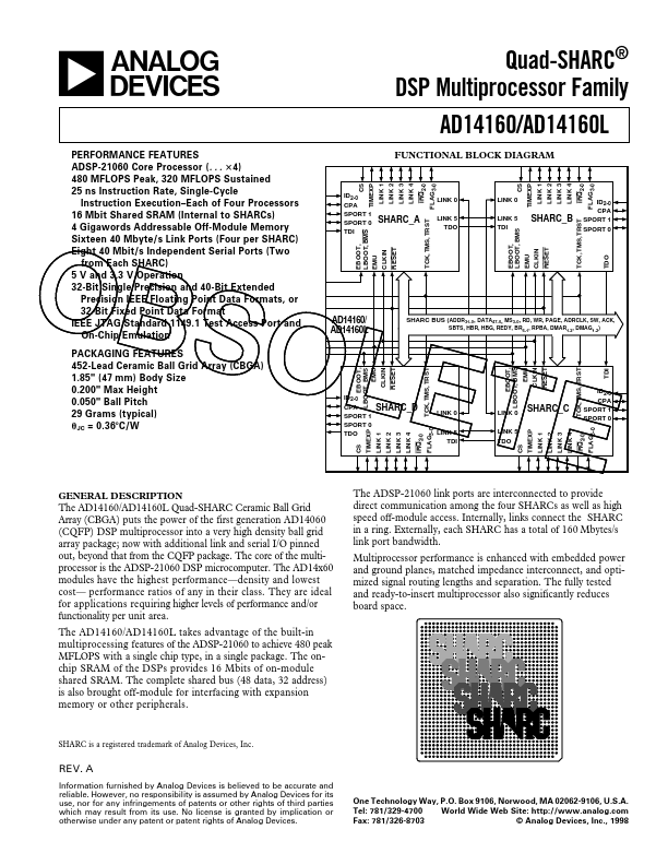
FUNCTIONAL BLOCK DIAGRAM ADSP-21060 Core Processor (. . . ؋4) 480 MFLOPS Peak, 320 MFLOPS Sustained CS TIMEXP LINK 1 LINK 2 LINK 3 LINK 4 IRQ2-0 FLAG3-0 CS TIMEXP LINK 1 LINK 2 LINK 3 LINK 4 IRQ2-0 FLAG3-0 25 ns Instruction Rate, Single-Cycle Instruction Execution–Each of Four Processors ID2-0 CPA LINK 0 LINK 0 ID2-0 EBOOT, LBOOT, BMS EMU CLKIN RESET TCK, TMS, TRST EBOOT, LBOOT, BMS EMU CLKIN RESET TCK, TMS, TRST 16 Mbit Shared SRAM (Internal to SHARCs) 4 Gigawords Addressable Off-Module Memory SPORT 1 SPORT 0 SHARC_A TDI LINK 5 TDO LINK 5 TDI CPA SHARC_B SPORT 1 SPORT 0 Sixteen 40 Mbyte/s Link Ports (Four per SHARC) Eight 40 Mbit/s Independent Serial Ports (Two from Each SHARC) 5 V and 3.3 V Operation 32-Bit Single Precision and 40-Bit Extended Precision IEEE Floating Point Data Formats, or O32-Bit Fixed Point Data Format IEEE JTAG Standard 1149.1 Test Access Port and BOn-Chip Emulation SPACKAGING FEATURES
452-Lead Ceramic Ball Grid Array (CBGA) O1.85" (47 mm) Body Size 0.200... Analog Devices