AD5684R
AD5684R is Quad 16-/14-/12-Bit nanoDAC manufactured by Analog Devices.
Data Sheet AD5686R/AD5685R/AD5684R
Quad, 16-/14-/12-Bit nano DAC+ with 2 ppm/°C Reference, SPI Interface
Features
- High relative accuracy (INL): ±2 LSB maximum at 16 bits
- Low drift 2.5 V reference: 2 ppm/°C typical
- Tiny package: 3 mm × 3 mm, 16-lead LFCSP
- Total unadjusted error (TUE): ±0.1% of FSR maximum
- Offset error: ±1.5 m V maximum
- Gain error: ±0.1% of FSR maximum
- High drive capability: 20 m A, 0.5 V from supply rails
- User selectable gain of 1 or 2 (GAIN pin)
- Reset to zero scale or midscale (RSTSEL pin)
- 1.8 V logic patibility
- 50 MHz SPI with readback or daisy chain
- Low glitch: 0.5 n V-sec
- Low power: 3.3 m W at 3 V
- 2.7 V to 5.5 V power supply
- - 40°C to +105°C temperature range
APPLICATIONS
- Optical transceivers
- Base-station power amplifiers
- Process control (PLC I/O cards)
- Industrial automation
- Data acquisition systems
GENERAL DESCRIPTION
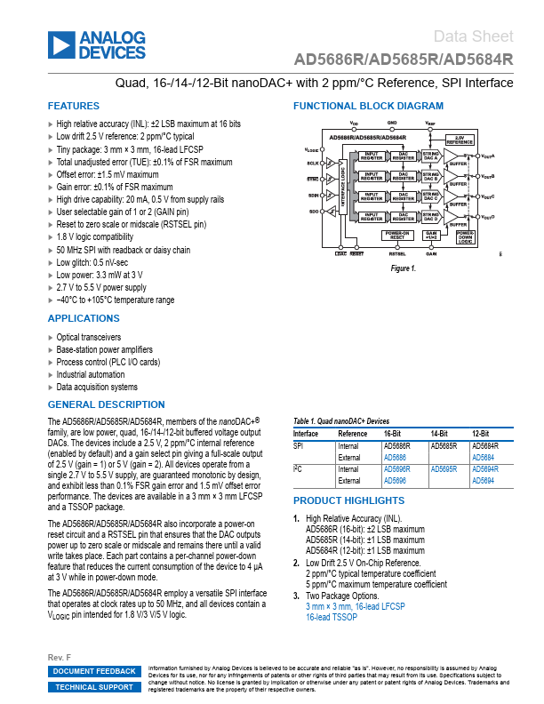
The AD5686R/AD5685R/AD5684R, members of the nano DAC+® family, are low power, quad, 16-/14-/12-bit buffered voltage output DACs. The devices include a 2.5 V, 2 ppm/°C internal reference (enabled by default) and a gain select pin giving a full-scale output of 2.5 V (gain = 1) or 5 V (gain = 2). All devices operate from a single 2.7 V to 5.5 V supply, are guaranteed monotonic by design, and exhibit less than 0.1% FSR gain error and 1.5 m V offset error performance. The devices are available in a 3 mm × 3 mm LFCSP and a TSSOP package.
The AD5686R/AD5685R/AD5684R also incorporate a power-on reset circuit and a RSTSEL pin that ensures that the DAC outputs power up to zero scale or midscale and remains there until a valid write takes place. Each part contains a per-channel power-down feature that reduces the current consumption of the device to 4 µA at 3 V while in power-down mode.
The AD5686R/AD5685R/AD5684R employ a versatile SPI interface that operates at clock rates up to 50 MHz, and all devices contain a VLOGIC pin intended for 1.8 V/3 V/5 V logic.
FUNCTIONAL BLOCK DIAGRAM
Figure...