Datasheet4U Logo Datasheet4U.com

AD5695R - Quad 16-/14-/12-Bit nanoDAC+

Download the AD5695R datasheet PDF. This datasheet also covers the AD5696R variant, as both devices belong to the same quad 16-/14-/12-bit nanodac+ family and are provided as variant models within a single manufacturer datasheet.

Description

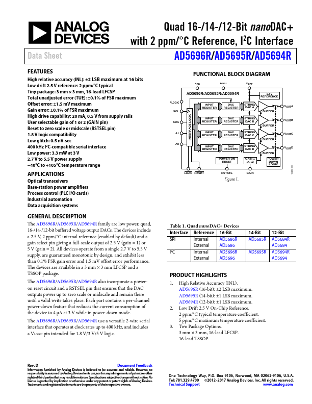
The AD5696R/AD5695R/AD5694R family are low power, quad, 16-/14-/12-bit buffered voltage output DACs.

The devices include a 2.5 V, 2 ppm/°C internal reference (enabled by default) and a gain select pin giving a full-scale output of 2.5 V (gain = 1) or 5 V (gain = 2).

Features

  • High relative accuracy (INL): ±2 LSB maximum at 16 bits Low drift 2.5 V reference: 2 ppm/°C typical Tiny package: 3 mm × 3 mm, 16-lead LFCSP Total unadjusted error (TUE): ±0.1% of FSR maximum Offset error: ±1.5 mV maximum Gain error: ±0.1% of FSR maximum High drive capability: 20 mA, 0.5 V from supply rails User selectable gain of 1 or 2 (GAIN pin) Reset to zero scale or midscale (RSTSEL pin) 1.8 V logic compatibility Low glitch: 0.5 nV-sec 400 kHz I2C-compatible serial interface Low power: 3.3.

📥 Download Datasheet

Note: The manufacturer provides a single datasheet file (AD5696R-AnalogDevices.pdf) that lists specifications for multiple related part numbers.

Full PDF Text Transcription

Click to expand full text
Data Sheet Quad 16-/14-/12-Bit nanoDAC+ with 2 ppm/°C Reference, I2C Interface AD5696R/AD5695R/AD5694R FEATURES High relative accuracy (INL): ±2 LSB maximum at 16 bits Low drift 2.5 V reference: 2 ppm/°C typical Tiny package: 3 mm × 3 mm, 16-lead LFCSP Total unadjusted error (TUE): ±0.1% of FSR maximum Offset error: ±1.5 mV maximum Gain error: ±0.1% of FSR maximum High drive capability: 20 mA, 0.5 V from supply rails User selectable gain of 1 or 2 (GAIN pin) Reset to zero scale or midscale (RSTSEL pin) 1.8 V logic compatibility Low glitch: 0.5 nV-sec 400 kHz I2C-compatible serial interface Low power: 3.3 mW at 3 V 2.7 V to 5.
Published: |