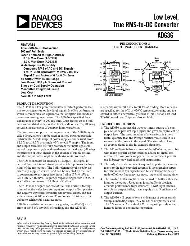
AD636
AD636 is Low Level/ True RMS-to-DC Converter manufactured by Analog Devices.
a
Features
True RMS-to-DC Conversion 200 m V Full Scale Laser-Trimmed to High Accuracy 0.5% Max Error (AD636K) 1.0% Max Error (AD636J) Wide Response Capability: putes RMS of AC and DC Signals 1 MHz
- 3 d B Bandwidth: V RMS >100 m V Signal Crest Factor of 6 for 0.5% Error d B Output with 50 d B Range Low Power: 800 A Quiescent Current Single or Dual Supply Operation Monolithic Integrated Circuit Low Cost Available in Chip Form PRODUCT DESCRIPTION
VIN 1 NC 2
- VS 3 CAV 4 d B 5 BUF OUT 6 BUF IN 7
Low Level, True RMS-to-DC Converter AD636
PIN CONNECTIONS & FUNCTIONAL BLOCK DIAGRAM
IOUT
ABSOLUTE VALUE 14 +VS 13 NC
10k⍀ + CURRENT MIRROR
BUF IN
- AD636
SQUARER DIVIDER
12 NC 11 NC
BUF OUT
10k⍀
CURRENT MIRROR + BUF
- 10k⍀ 10k⍀
10 MON 9 8
+VS
SQUARER DIVIDER ABSOLUTE VALUE d B
RL IOUT VIN
- VS
NC = NO CONNECT
The AD636 is a low power monolithic IC which performs true rms-to-dc conversion on low level signals. It offers performance which is parable or superior to that of hybrid and modular converters costing much more. The AD636 is specified for a signal range of 0 m V to 200 m V rms. Crest factors up to 6 can be acmodated with less than 0.5% additional error, allowing accurate measurement of plex input waveforms. The low power supply current requirement of the AD636, typically 800 µA, allows it to be used in battery-powered portable instruments. A wide range of power supplies can be used, from ± 2.5 V to ± 16.5 V or a single +5 V to +24 V supply. The input and output terminals are fully protected; the input signal can exceed the power supply with no damage to the device (allowing the presence of input signals in the absence of supply voltage) and the output buffer amplifier is short-circuit protected. The AD636 includes an auxiliary d B output. This signal is derived from an internal circuit point which represents the logarithm of the rms output. The 0 d B reference level is set by an externally supplied current and can be...