AD9481
AD9481 is A/D Converter manufactured by Analog Devices.
Features
DNL = ±0.35 LSB INL = ±0.26 LSB Single 3.3 V supply operation (3.0 V to 3.6 V) Power dissipation of 439 m W at 250 MSPS 1 V p-p analog input range Internal 1.0 V reference Single-ended or differential analog inputs De-multiplexed CMOS outputs Power-down mode Clock duty cycle stabilizer
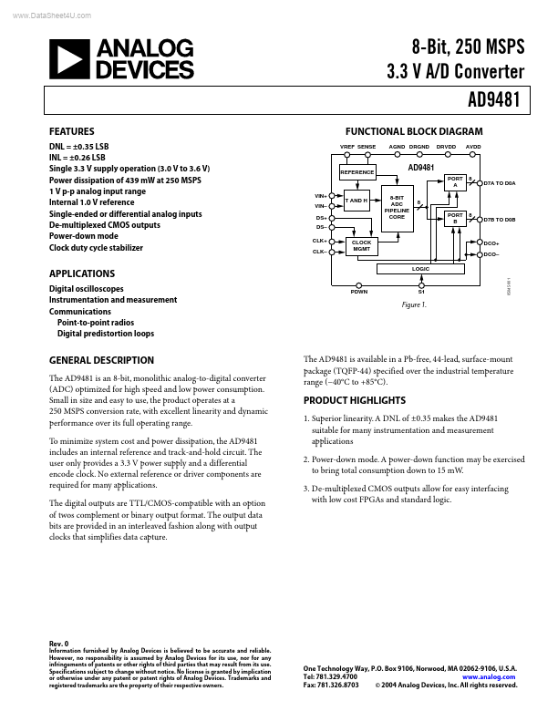
FUNCTIONAL BLOCK DIAGRAM
VREF SENSE AGND DRGND DRVDD AVDD
REFERENCE
PORT A 8 D7A TO D0A
VIN+ VIN- DS+ DS- CLK+ CLK-
T AND H
8-BIT ADC PIPELINE CORE
8 PORT B 8 D7B TO D0B
CLOCK MGMT
DCO+ DCO- LOGIC
05045-001
APPLICATIONS
Digital oscilloscopes Instrumentation and measurement munications Point-to-point radios Digital predistortion loops
PDWN
S1
Figure 1.
GENERAL DESCRIPTION
The AD9481 is an 8-bit, monolithic analog-to-digital converter (ADC) optimized for high speed and low power consumption. Small in size and easy to use, the product operates at a 250 MSPS conversion rate, with excellent linearity and dynamic performance over its full operating range. To minimize system cost and power dissipation, the AD9481 includes an internal reference and track-and-hold circuit. The user only provides a 3.3 V power supply and a differential encode clock. No external reference or driver ponents are required for many applications. The digital outputs are TTL/CMOS-patible with an option of twos plement or binary output format. The output data bits are provided in an interleaved fashion along with output clocks that simplifies data capture.
The AD9481 is available in a Pb-free, 44-lead, surface-mount package (TQFP-44) specified over the industrial temperature range (- 40°C to +85°C).
PRODUCT HIGHLIGHTS
1. Superior linearity. A DNL of ±0.35 makes the AD9481 suitable for many instrumentation and measurement applications 2. Power-down mode. A power-down function may be exercised to bring total consumption down to 15 m W. 3. De-multiplexed CMOS outputs allow for easy interfacing with low cost FPGAs and standard logic.
Rev. 0
Information furnished by Analog Devices is believed...