AD9484
AD9484 is 1.8 V Analog-to-Digital Converter manufactured by Analog Devices.
Features
SNR = 47 d BFS at f IN up to 250 MHz at 500 MSPS ENOB of 7.5 bits at f IN up to 250 MHz at 500 MSPS (- 1.0 d BFS) SFDR = 79 d Bc at f IN up to 250 MHz at 500 MSPS (- 1.0 d BFS) Integrated input buffer Excellent linearity DNL = ±0.1 LSB typical INL = ±0.1 LSB typical LVDS at 500 MSPS (ANSI-644 levels) 1 GHz full power analog bandwidth On-chip reference, no external decoupling required Low power dissipation 670 m W at 500 MSPS- LVDS SDR output Programmable (nominal) input voltage range 1.18 V p-p to 1.6 V p-p, 1.5 V p-p nominal 1.8 V analog and digital supply operation Selectable output data format (offset binary, twos plement, Gray code) Clock duty cycle stabilizer Integrated data capture clock
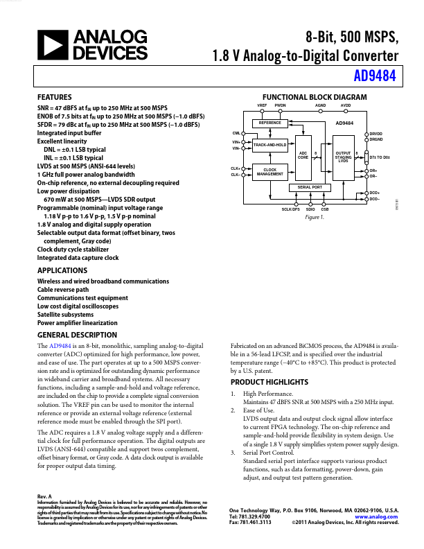
FUNCTIONAL BLOCK DIAGRAM
VREF PWDN AGND AVDD
REFERENCE CML VIN+ VIN- TRACK-AND-HOLD ADC CORE CLK+ CLK- 8
DRVDD DRGND
OUTPUT STAGING LVDS
8 D7± TO D0±
CLOCK MANAGEMENT
OR+ OR- SERIAL PORT DCO+
09615-001
DCO- SCLK/DFS SDIO CSB
Figure 1.
APPLICATIONS
Wireless and wired broadband munications Cable reverse path munications test equipment Low cost digital oscilloscopes Satellite subsystems Power amplifier linearization
GENERAL DESCRIPTION
The AD9484 is an 8-bit, monolithic, sampling analog-to-digital converter (ADC) optimized for high performance, low power, and ease of use. The part operates at up to a 500 MSPS conversion rate and is optimized for outstanding dynamic performance in wideband carrier and broadband systems. All necessary functions, including a sample-and-hold and voltage reference, are included on the chip to provide a plete signal conversion solution. The VREF pin can be used to monitor the internal reference or provide an external voltage reference (external reference mode must be enabled through the SPI port). The ADC requires a 1.8 V analog voltage supply and a differential clock for full performance operation. The digital outputs are LVDS (ANSI-644) patible and support twos plement, offset binary format, or Gray code. A data clock output is...