FEATURES
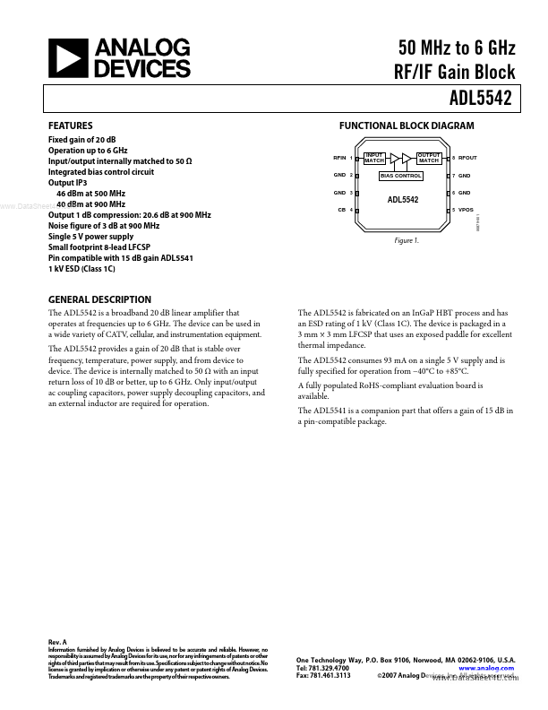
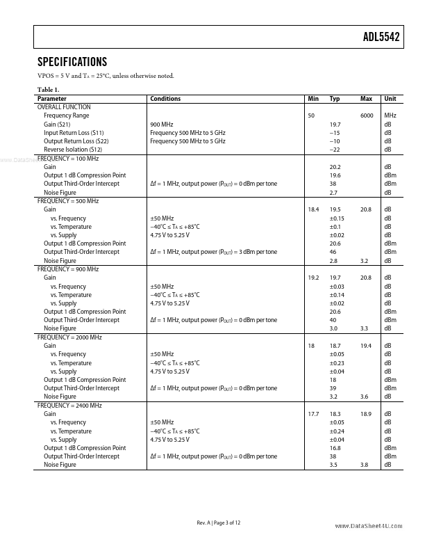
Fixed gain of 20 dB Operation up to 6 GHz Input/output internally matched to 50 Ω Integrated bias control circuit Output IP3 46 dBm at 500 MHz 40 dBm at 900 MHz Output 1 dB compression: 20.6 dB at 900 MHz Noise figure of 3 dB at 900 MHz Single 5 V power supply Small footprint 8-lead LFCSP Pin compatible with 15 dB gain ADL5541 1 kV ESD (Class 1C) FUNCTIONAL BLOCK DIAGRAM INPUT MATCH OUTPUT MATCH RFIN 1 GND 2 GND 3 8 RFOUT GND GND VPOS 06879-001 BIAS CONTROL 7 6 ADL5542 CB 4 5 Figure 1. GENERAL DESCRIPTION
The device is internally matched to 50 Ω with an input return loss of 10 dB or better, up to 6 GHz. Only input/output ac coupling capacitors, power supply decoupling capacitors, and an external inductor are required for operation. The ADL5542 is fabricated on an InGaP HBT process and has an ESD rating of 1 kV (Class 1C). The device is packaged in a 3 mm × 3 mm LFCSP that uses an exposed paddle for excellent thermal impedance. The ADL5542 consumes 93 mA on a single 5 V supply and is fully specified for operation from −40°C to +85°C. Analog Devices