FEATURES
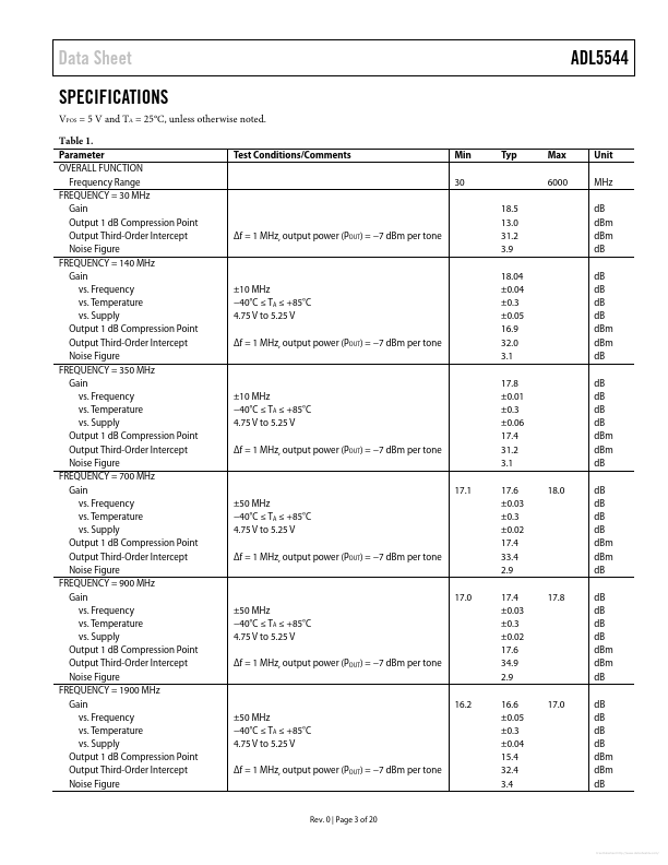
Fixed gain of 17.4 dB Broadband operation from 30 MHz to 6 GHz Input/output internally matched to 50 Ω Integrated bias control circuit OIP3 of 34.9 dBm at 900 MHz P1dB of 17.6 dBm at 900 MHz Noise figure of 2.9 dB at 900 MHz Single 5 V power supply Low quiescent current of 55 mA Wide operating temperature range of −40°C to +105°C Thermally efficient SOT-89 package ESD rating of ±1.5 kV (Class 1C) 30 MHz to 6 GHz RF/IF Gain Block ADL5544 FUNCTIONAL BLOCK DIAGRAM GND (2) ADL5544 BIAS 1 2 3 11384-001 RFIN GND RFOUT Figure 1. GENERAL DESCRIPTION
The amplifier is offered in the industry-standard SOT-89 package and is internally matched to 50 Ω at the input and output, making the ADL5544 very easy to implement in a wide variety of applications. The only external components required are the input/output ac coupling capacitors, power supply decoupling capacitors, and dc bias inductor. The ADL5544 is fabricated on an InGaP HBT process and has a high ESD rating of ±1.5 kV (Class 1C). The ADL5544 is also fully specified for operation across the wide temperature range of −40°C to +105°C. Analog Devices