ADN2892
ADN2892 is Limiting Amplifier manufactured by Analog Devices.
FEATURES
SFP reference design available Input sensitivity: 3 m V p-p 65 ps rise/fall times BW Select to support Multi-Rate 1x/2x/4x FC modules Optional LOS Output Inversion to support SFF CML outputs: 700 m V p-p differential Programmable LOS detector: 3 m V to 45 m V Rx signal strength indicator (RSSI): SFF-8472 pliant average power measurement Single supply operation: 3.3 V Low power dissipation: 160 m W Available in space-saving 3 × 3 mm 16-lead LFCSP Increased Temperature Range: -40o C to 95o C
3.3 V 4.25 Gb/s Limiting Amplifier ADN2892
The ADN2892 is a high gain, limiting amplifier optimized for use in Fibre Channel and Gb E optical receivers. The ADN2892 accepts input levels of up to 2.0 V p-p differential and has 3 m V p-p differential input sensitivity. The ADN2892 provides the receiver functions of quantization and loss of signal (LOS) detection. The ADN2892 has an on-chip selectable filter to reduce the BW of the limamp to 1.5GHz in order to filter out the relaxation oscillation of legacy 1Gb/s Fiber Channel transmitters with CD lasers. The reduced BW will also allow for more optical Rx sensitivity margin at the lower data rates such as 1x FC and 1Gb E in multi-rate modules. The limiting amplifier also measures average received power based on a direct measurement of the photodiode current with better than 1 d B of accuracy over the entire input range of the receiver. This eliminates the need for external average Rx power detection circuitry in SFF-8472 pliant optical transceivers. The ADN2892 limiting amplifier operates from a single 3.3 V supply, has low power dissipation, and is available in a spacesaving 3 × 3 mm 16-lead lead frame chip scale package (LFCSP).
APPLICATIONS
SFP/SFF/GBIC optical transceivers 1x/2x/4x Multi-rate Fibre Channel receivers LX4 WDM transponders
PRODUCT OVERVIEW
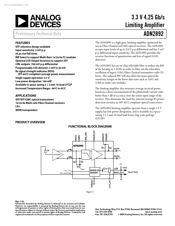
FUNCTIONAL BLOCK DIAGRAM
ADN2882
+V
PD_VCC PD_CATHODE VREF
10kΩ ADu C7020
Figure 1.
Rev. Pr A.
Information furnished by Analog Devices is believed to be accurate and reliable....