ADP1765
ADP1765 is CMOS Linear Regulator manufactured by Analog Devices.
FEATURES
5 A maximum output current Low input voltage supply range
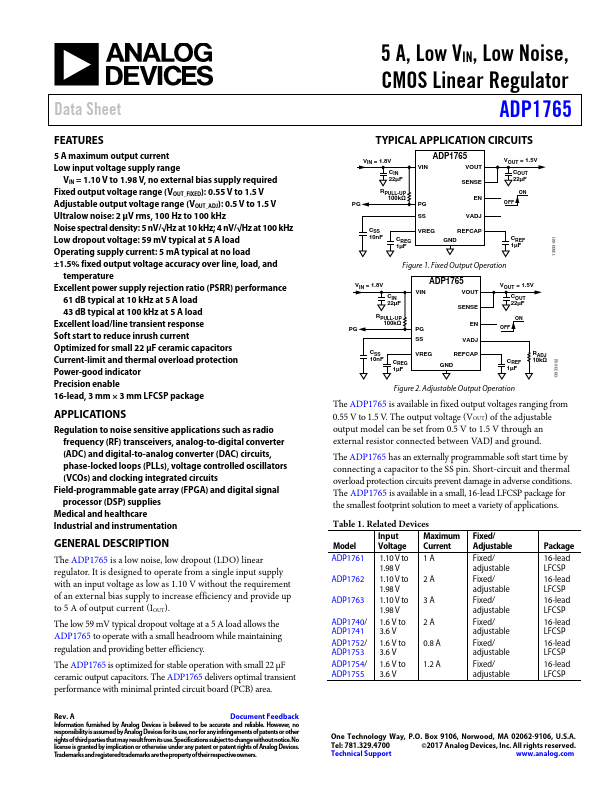
VIN = 1.10 V to 1.98 V, no external bias supply required Fixed output voltage range (VOUT_FIXED): 0.55 V to 1.5 V Adjustable output voltage range (VOUT_ADJ): 0.5 V to 1.5 V Ultralow noise: 2 µV rms, 100 Hz to 100 k Hz Noise spectral density: 5 n V/√Hz at 10 k Hz; 4 n V/√Hz at 100 k Hz Low dropout voltage: 59 m V typical at 5 A load Operating supply current: 5 m A typical at no load ±1.5% fixed output voltage accuracy over line, load, and temperature Excellent power supply rejection ratio (PSRR) performance
61 d B typical at 10 k Hz at 5 A load 43 d B typical at 100 k Hz at 5 A load Excellent load/line transient response Soft start to reduce inrush current Optimized for small 22 µF ceramic capacitors Current-limit and thermal overload protection Power-good indicator Precision enable 16-lead, 3 mm × 3 mm LFCSP package
APPLICATIONS
Regulation to noise sensitive applications such as radio frequency (RF) transceivers, analog-to-digital converter (ADC) and digital-to-analog converter (DAC) circuits, phase-locked loops (PLLs), voltage controlled oscillators (VCOs) and clocking integrated circuits
Field-programmable gate array (FPGA) and digital signal processor (DSP) supplies
Medical and healthcare Industrial and instrumentation
GENERAL DESCRIPTION
The ADP1765 is a low noise, low dropout (LDO) linear regulator. It is designed to operate from a single input supply with an input voltage as low as 1.10 V without the requirement of an external bias supply to increase efficiency and provide up to 5 A of output current (IOUT).
The low 59 m V typical dropout voltage at a 5 A load allows the ADP1765 to operate with a small headroom while maintaining regulation and providing better efficiency.
The ADP1765 is optimized for stable operation with small 22 µF ceramic output capacitors. The ADP1765 delivers optimal transient performance with minimal printed circuit board (PCB) area.
Rev. A
Document Feedback
Information furnished...